Skip to content
简体中文
繁體中文
日本語
Asia – English
language
Samco Inc.
USA Website Next Gen
Products
Deposition Systems
Atomic Layer Deposition (ALD)
Anode PECVD
Cathode PECVD
Etching Systems
Atomic Layer Etching (ALE)
Inductively Coupled Plasma (ICP) Etching
Si Deep Reactive Ion Etching (DRIE)
Reactive Ion Etching (RIE) – Plasma Etching
Xenon Difluoride (XeF2) Etching
Surface Treatment Systems
Aqua Plasma®
Plasma Cleaning
UV Ozone Cleaning
Processes
Deposition
Atomic Layer Deposition (ALD)
Anode PECVD
Cathode PECVD
Etching
Atomic Layer Etching (ALE)
Compound Semiconductor Etching
GaN Etching
GaAs Etching
InP Etching
Silicon Etching & DRIE
Metal/Dielectric Etching
Failure Analysis
Surface Treatment
Aqua Plasma®
Plasma Cleaning
UV Ozone Cleaning
Markets
News & Events
Events
News
Technical Reports
Interviews
Tutorials
Disclosure
About
Company Overview
Global Locations
History
Contact
Product Info Request
Technical Support Request
Careers
Search:
Products
Deposition Systems
Atomic Layer Deposition (ALD)
Anode PECVD
Cathode PECVD
Etching Systems
Atomic Layer Etching (ALE)
Inductively Coupled Plasma (ICP) Etching
Si Deep Reactive Ion Etching (DRIE)
Reactive Ion Etching (RIE) – Plasma Etching
Xenon Difluoride (XeF2) Etching
Surface Treatment Systems
Aqua Plasma®
Plasma Cleaning
UV Ozone Cleaning
Processes
Deposition
Atomic Layer Deposition (ALD)
Anode PECVD
Cathode PECVD
Etching
Atomic Layer Etching (ALE)
Compound Semiconductor Etching
GaN Etching
GaAs Etching
InP Etching
Silicon Etching & DRIE
Metal/Dielectric Etching
Failure Analysis
Surface Treatment
Aqua Plasma®
Plasma Cleaning
UV Ozone Cleaning
Markets
News & Events
Events
News
Technical Reports
Interviews
Tutorials
Disclosure
About
Company Overview
Global Locations
History
Contact
Product Info Request
Technical Support Request
Careers
News & Events
You are here:
Home
News & Events
Events
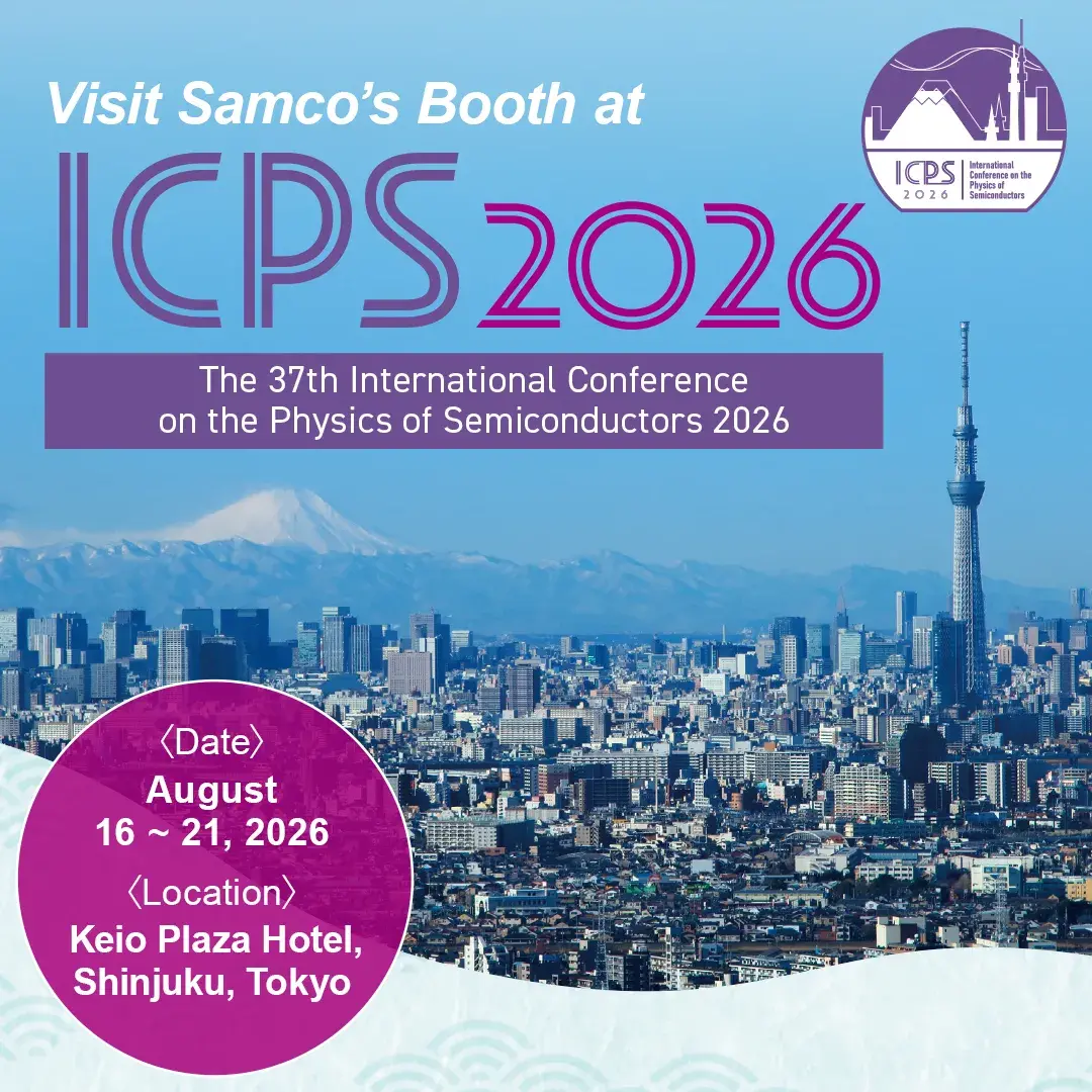
ICPS 2026
Date
August 16, 2026
–
August 21, 2026
Location
Keio Plaza Hotel, Shinjuku, Tokyo
All Events
Latest News
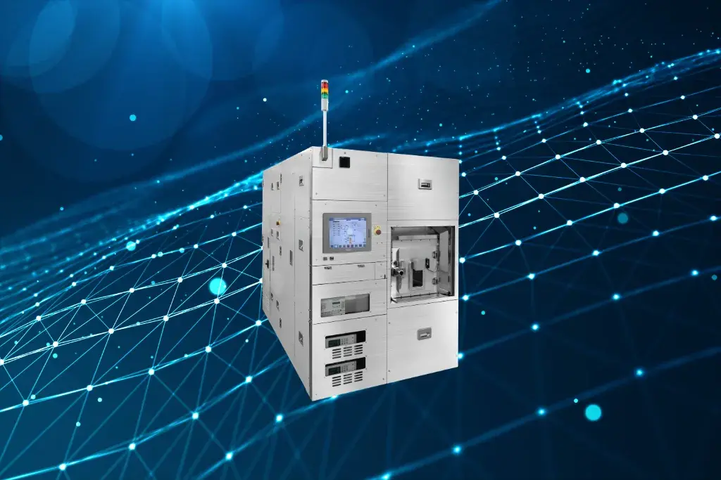
DTU Nanolab Expands Silicon DRIE Infrastructure with Etch System
News
May 26, 2026
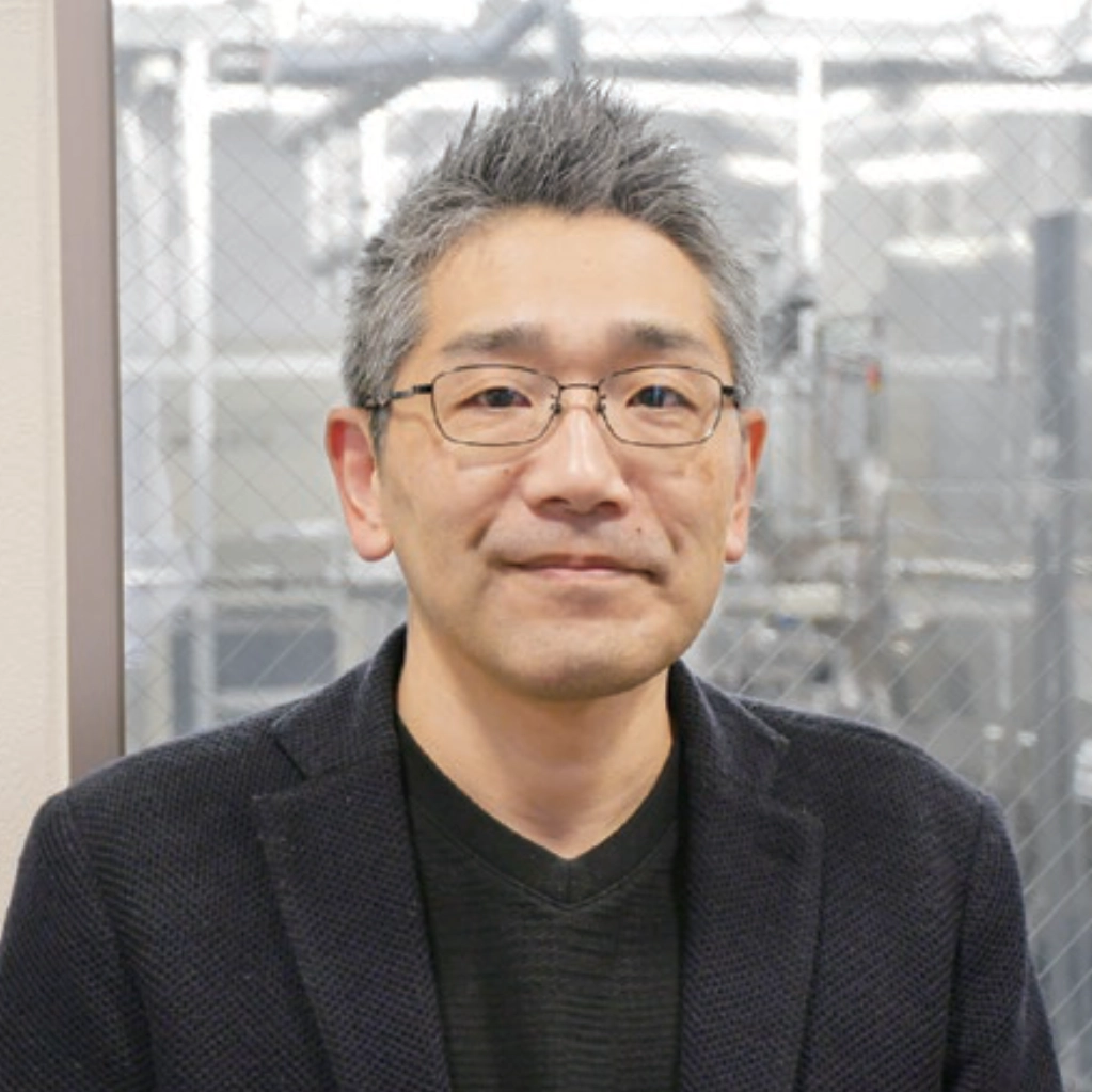
Tohoku University: Professor Mikihiko Oogane
Interviews
May 22, 2026
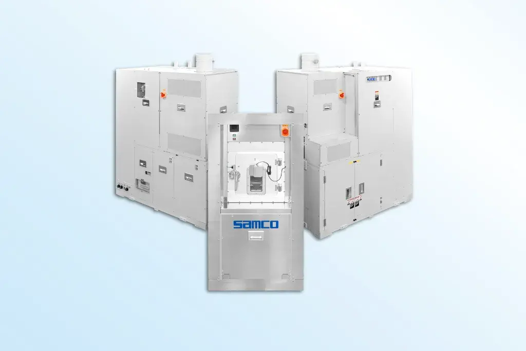
Introduction to the Dual-Chamber ALD System AD-8002LPC
Technical reports
May 22, 2026
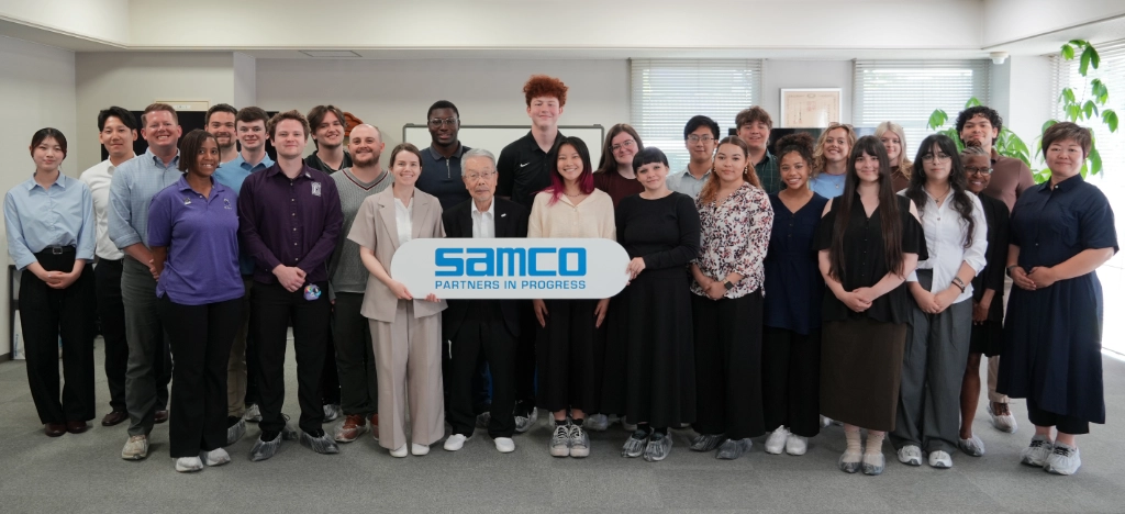
University of Central Arkansas Students Visit Samco Production Facility
News
May 20, 2026
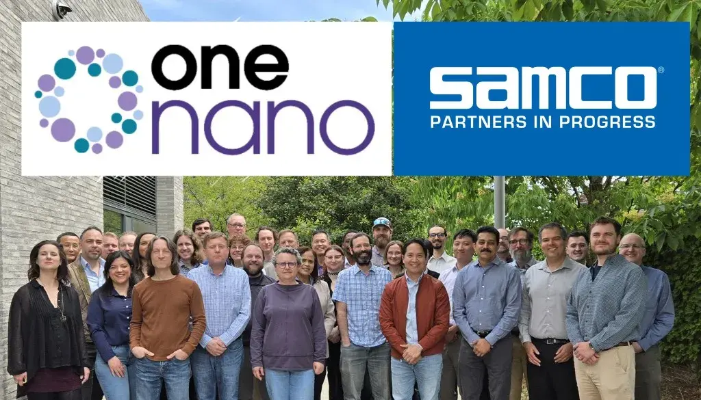
Samco Presents ALE Technologies at OneNano Mid-Atlantic Meeting
News
May 12, 2026
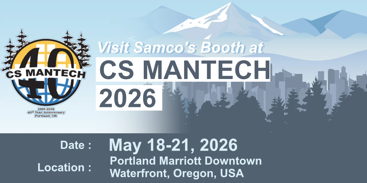
Samco to Exhibit at CS MANTECH 2026 in Portland
News
May 5, 2026
All News
News Categories
News
Events
Disclosure
Technical reports
Interviews
Tutorials
Go to Top