Patterned Sapphire Substrate & GaN Etch for HB LEDs
SAMCO Inc. > Featured Solutions > Sapphire/GaN Etch for HB LEDs
High-Brightness Light-Emitting-Diodes (HB LEDs)
Light Emitting Diodes (LEDs) have been widely used as lighting and displays. It is considered that the devices are key to save energy in growing population. However, the LED lighting is still expensive compared to conventional fluorescent lamp and incandescent lamp. Also, improvement of energy conversion efficiency with development of device fabrication technology is required.
As a pioneer of material processing, Samco offers Sapphire and GaN process solutions for High Brightness LED (HB LED) production, using experienced dry etching technology.


Samco’s Process Capabilities
Patterned Sapphire Substrate (PSS) Etching
Patterned Sapphire Substrates (PSS) are fabricated and used in GaN-based LEDs in order to increase the internal quantum efficiency by reducing GaN crystal defects. They also can improve external quantum efficiency by increasing the reflection area.


Regarding electroluminescence (EL) intensity, performing PSS etching improves the luminous efficiency by about 13% compared to processing without PSS. Therefore, PSS fabrication is one of the key processes for LED manufacturing. PSS shape, aspect ratio, and pattern density are important factors to improve the light extraction.
One challenge in PSS fabrication derives from sapphire’s material properties. The material is a very hard and chemically resistant material. Some LED manufactures use wet etch process because it is very fast and less expensive process. However, it is not easy to control the PSS profile precisely.
Samco offers dry etch processes for PSS fabrication using chlorine chemistry.


The PSS cone profile is highly controllable in height and width depending on customers’ requests.
Square pyramid and dome profile are also available.

Sidewall Angle: 41°

Sidewall Angle: 55°

Sidewall Angle: 61°
GaN Plasma Etching for Device Isolation
Samco offers GaN plasma etching solutions to improve the external luminous efficiency by preventing light escaping via the sidewalls.
A reverse-tapered etch process of GaNwas developed using chlorine chemistry.

Reverse-tapered Angle : 70°

Etch Rate : 140 nm/min (using a Ni mask)

Reverse-tapered GaN layer on Patterned Sapphire Substrate (PSS)
The Value of Samco’s Processes


Customer-proven solutions
Samco has provided dry etch solutions to world-leading LED manufacturers in East Asia.
Controllable and repeatable processes
Samco’s controllable and repeatable processes will improve productivity at LED fabs.
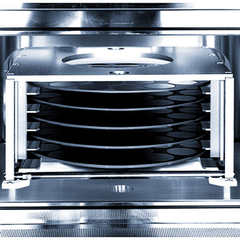
Throughput enhancement with batch processing
Samco offers batch processing solutions of sapphire wafers including ø4” and ø6”. The batch processing using a carrier enhances throughput of PSS fabrication.


Customer Publication
HB LED fabrication is one of Samco’s proprietary fields for both device industry and academia.
System Lineup