DTU Nanolab Expands Silicon DRIE Infrastructure with Etch System
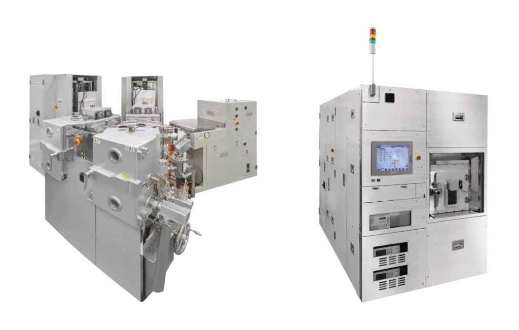
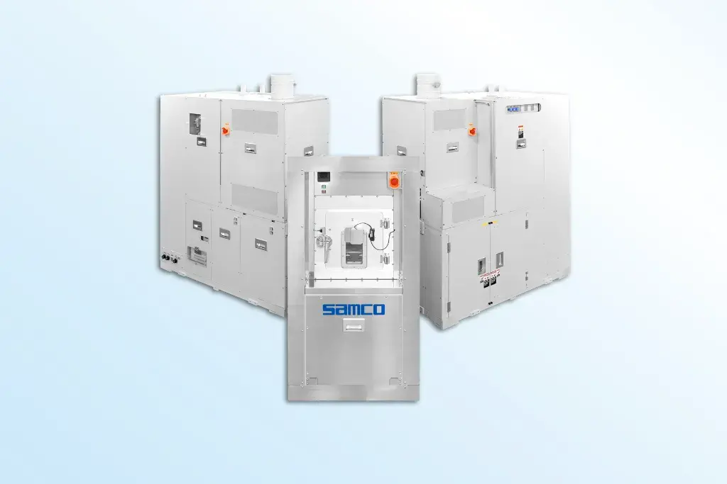
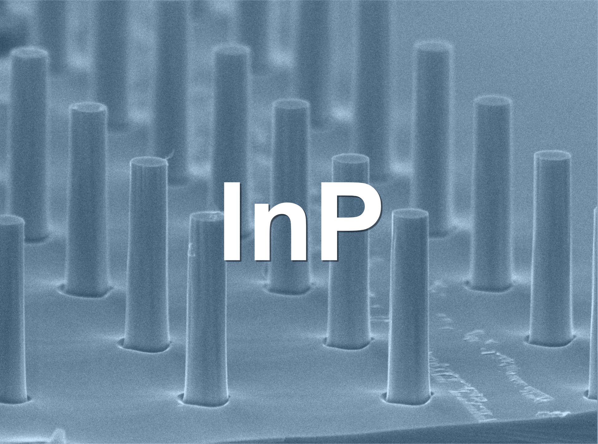
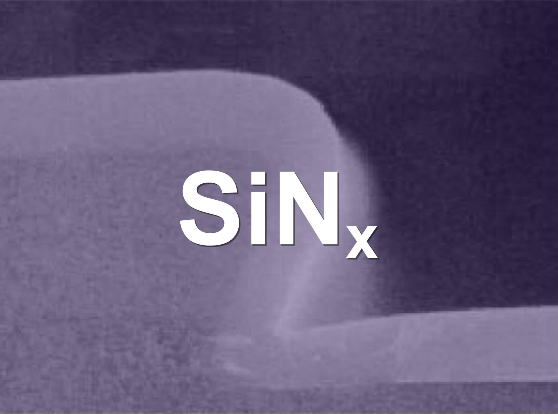
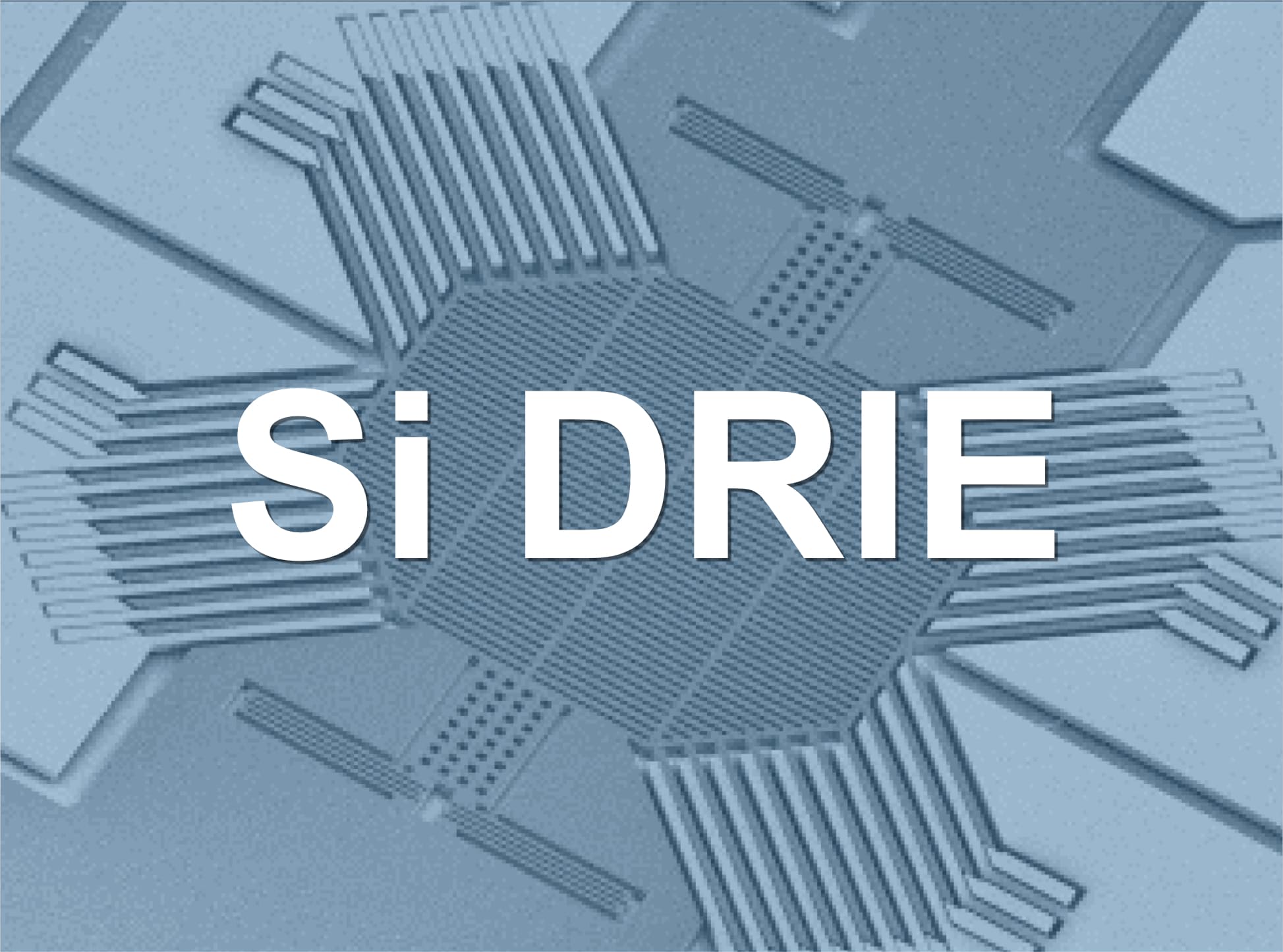
DTU Nanolab, Denmark’s national nanofabrication facility, will expand its silicon DRIE infrastructure with Samco’s cassette-loading RIE-800iPBC system to support advanced…


Established in 1979, Samco began as a garage start-up in Kyoto, aiming to provide cutting-edge semiconductor device and electronic component manufacturing systems globally. Over time, we have evolved into a leading global corporation with state-of-the-art technological capabilities and a widespread international presence. Our commitment to growth prioritizes “thin-film technology” as our core expertise.
DTU Nanolab, Denmark’s national nanofabrication facility, will expand its silicon DRIE infrastructure with Samco’s cassette-loading RIE-800iPBC system to support advanced…
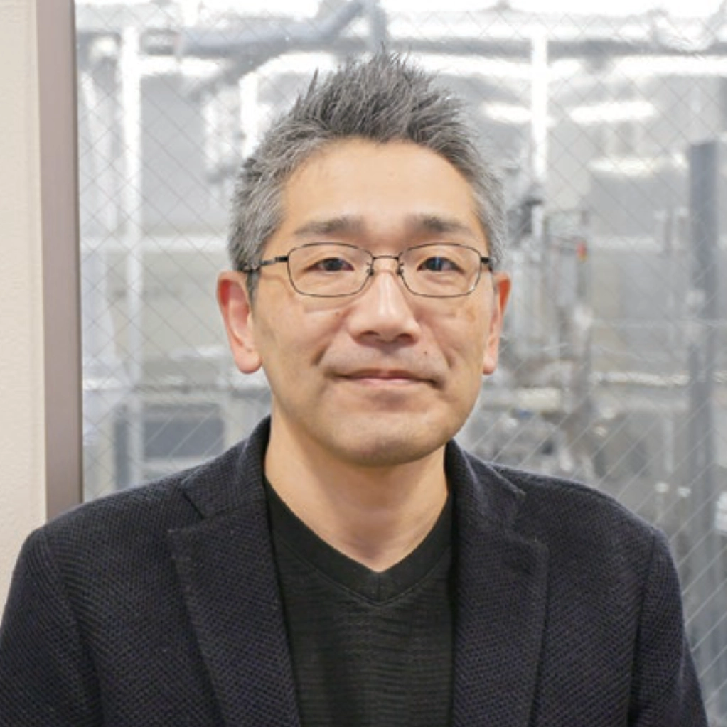
Professor Mikihiko Oogane discusses TMR sensors, quantum spintronics, and brain–information interfaces in magnetic sensing research at Tohoku University.
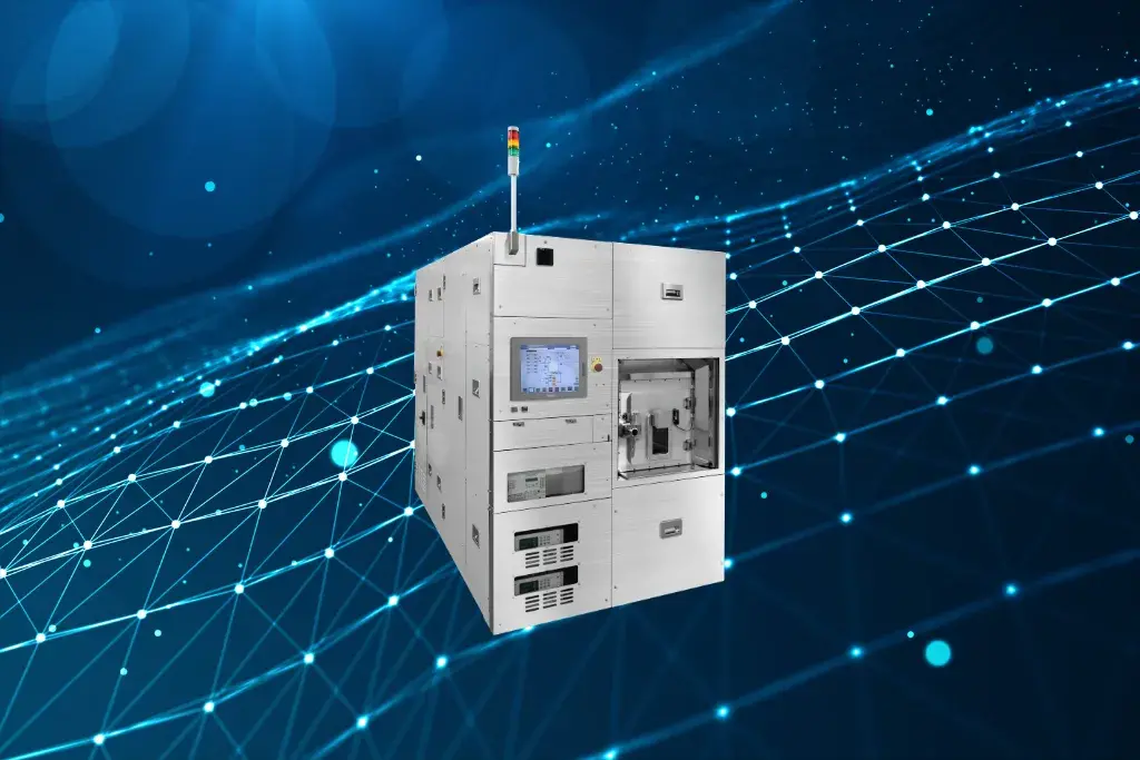
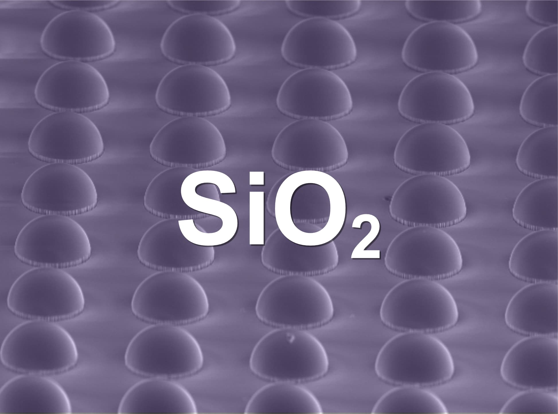
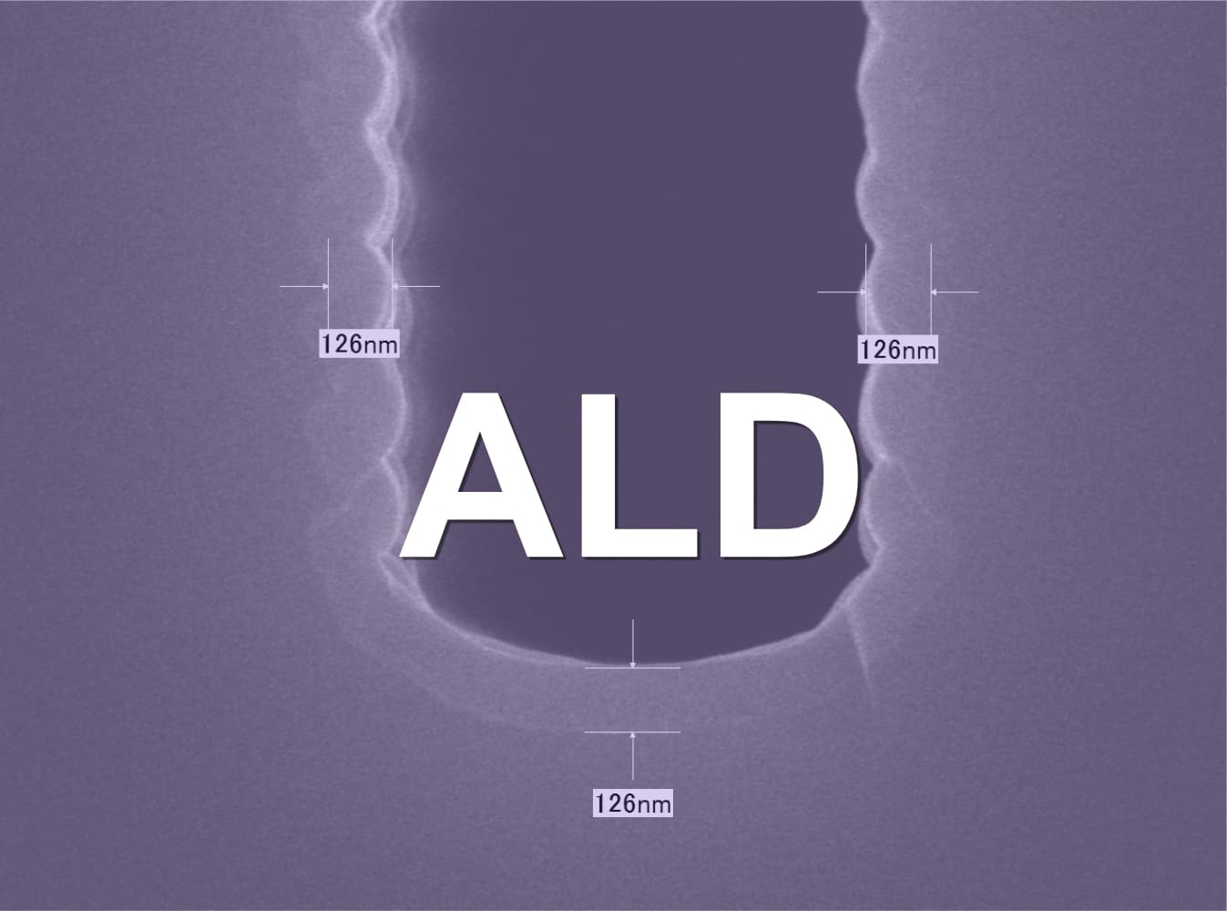
Samco’s AD-8002LPC dual-chamber ALD system enables stable TiOx deposition, reduced takt time, and flexible thermal and plasma ALD processing.
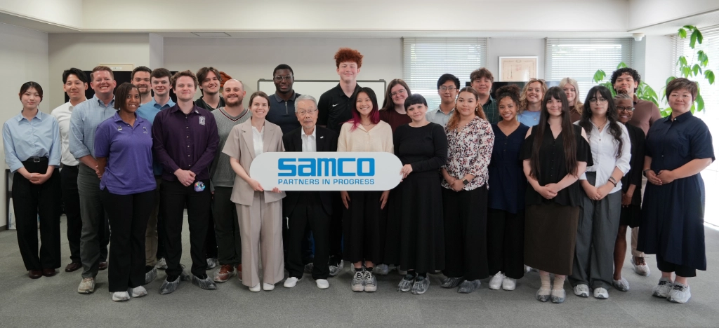
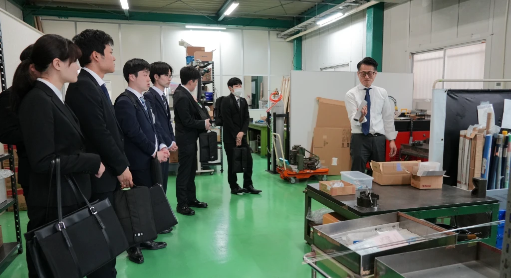
UCA students visit Samco to learn about semiconductors, plasma processing, Japanese business, and Samco’s founding story.
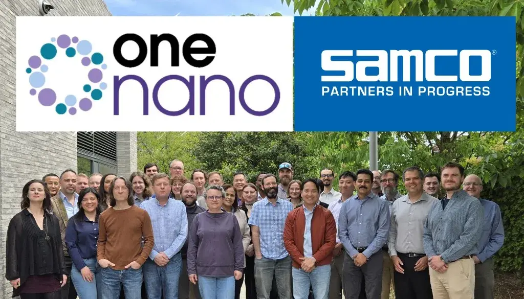
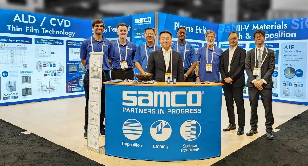
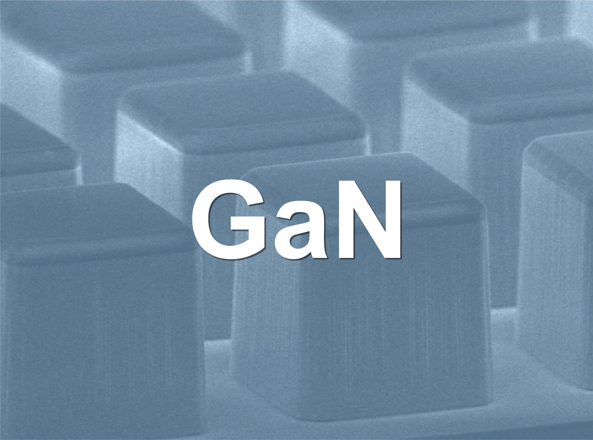
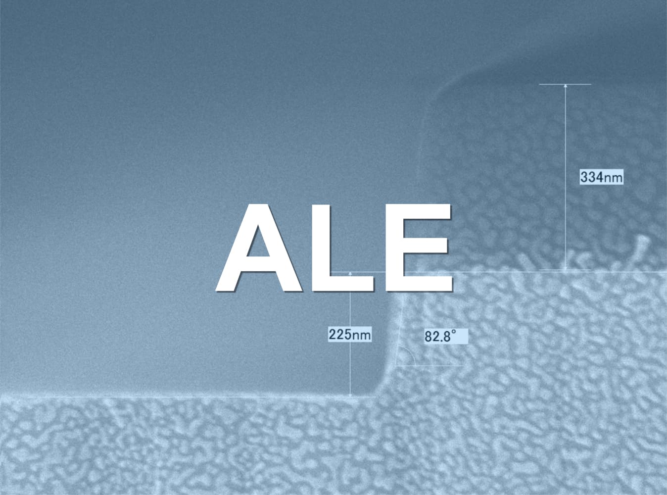
Samco presented ALE technologies at OneNano’s Spring Meredith Meeting, highlighting plasma-assisted etching for GaN HEMTs, diamond, and nanoscale devices.
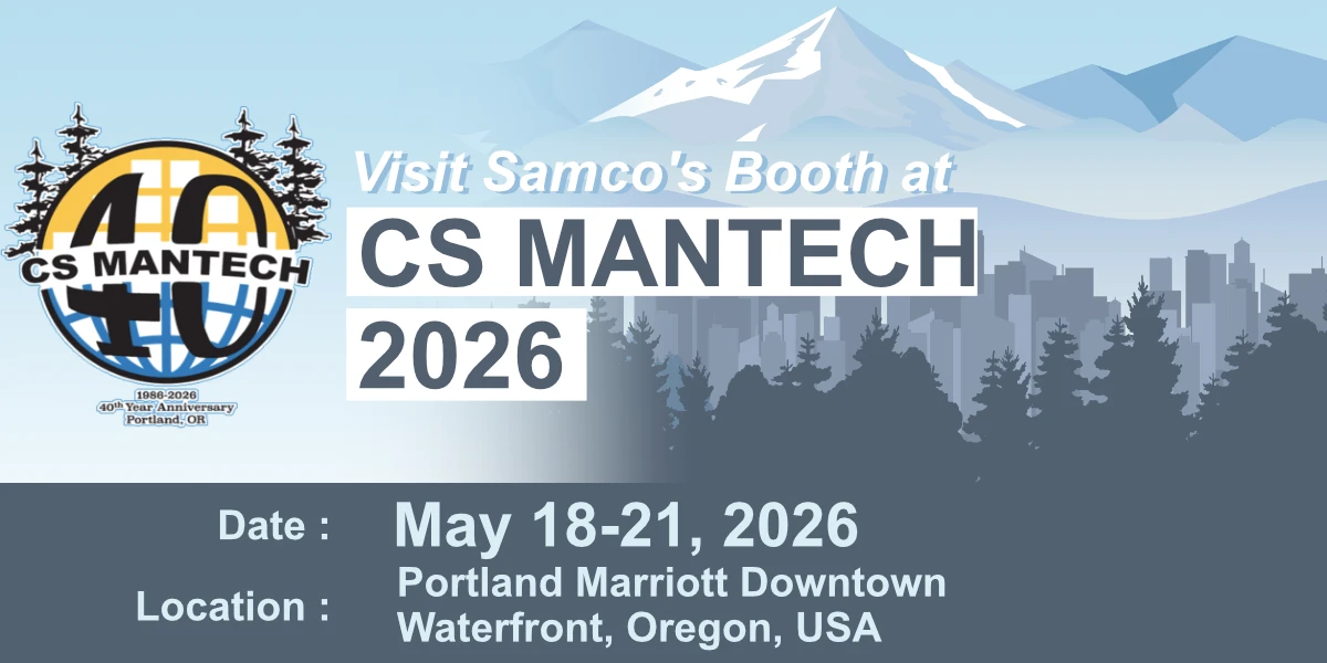
Samco Inc. will exhibit at CS MANTECH 2026, taking place from May 18–21, 2026, at the Portland Marriott Downtown Waterfront…
New employees visited Taisei Weld and Ushikoshi to learn how precision welding and metal fabrication support Samco’s semiconductor systems.
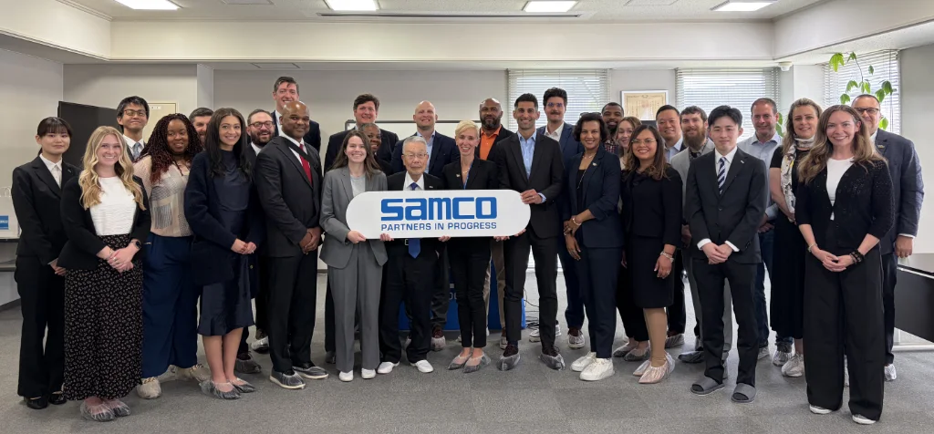
VCU EMBA students visited Samco in Kyoto, exploring its history, semiconductor manufacturing processes, and unique Kyoto approach to business and…
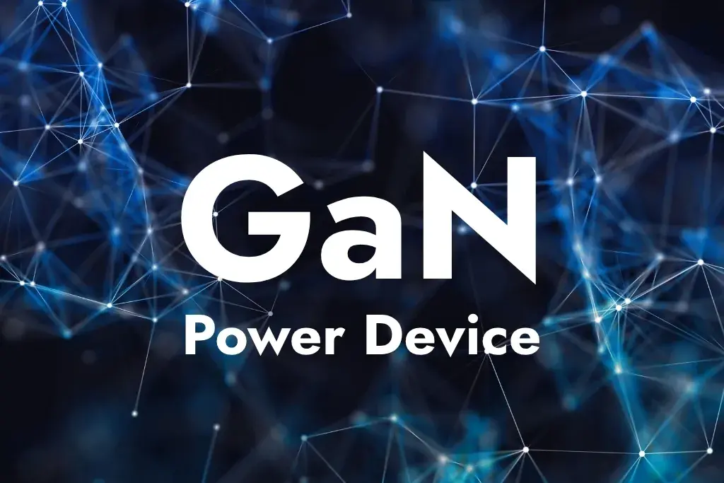
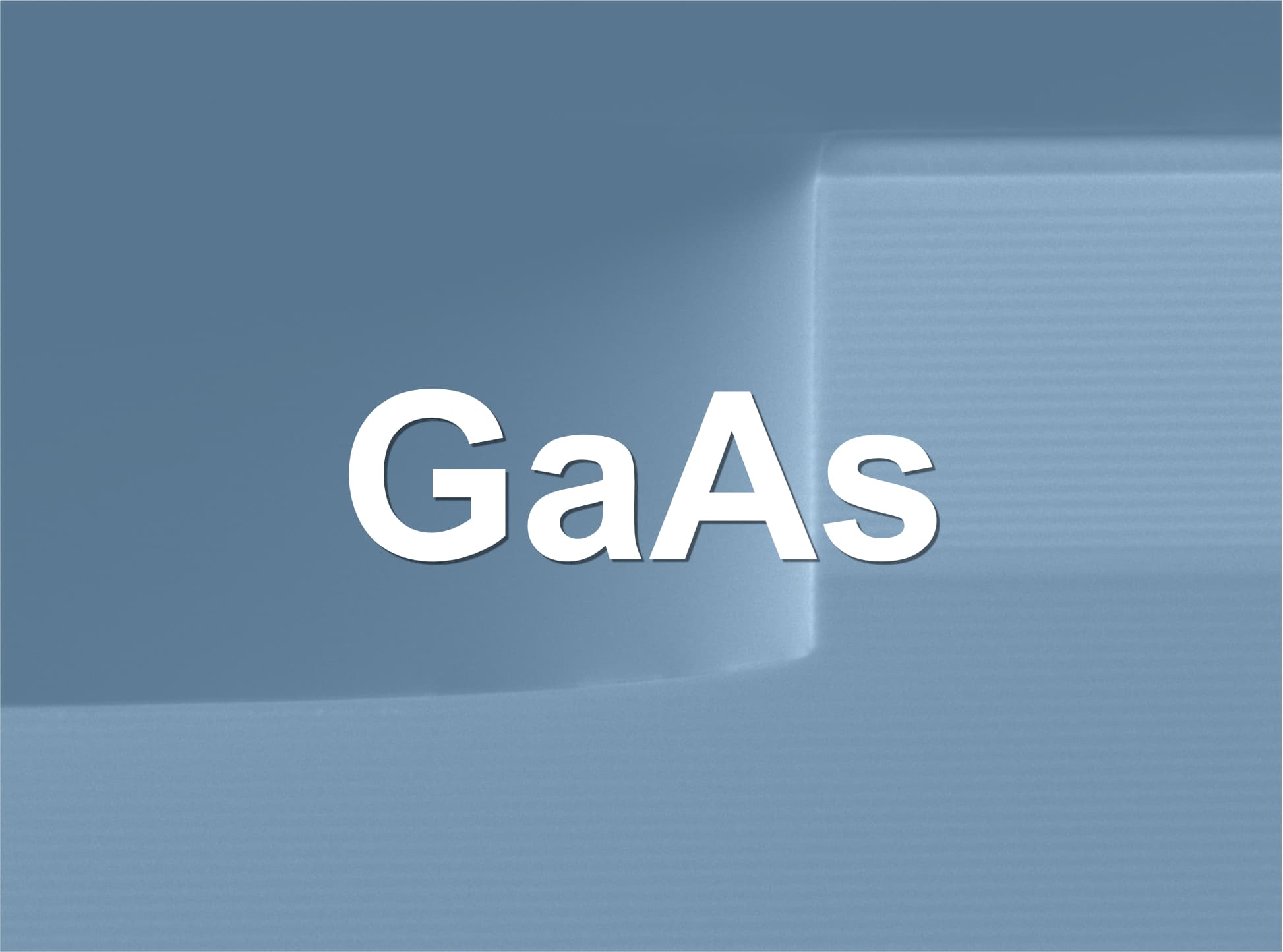
Samco systems support IMiF’s GaN pilot line, enabling precise AlGaN/GaN etching and advancing wide bandgap semiconductor research in Europe.
We deliver cutting-edge process equipment designed for precise film deposition, high-performance etching, and efficient surface cleaning. Our solutions cater to both R&D and production needs across diverse applications, including compound semiconductors, quantum computing, optoelectronics, MEMS, microfluidics, power devices, RF devices, and more.