


Sep.
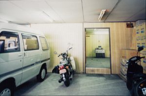
Samco International, Inc. was established
Jul.
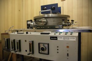
Released large CVD system for semiconductor process
Apr.
Released Japan’s first MOCVD system
Jun.
Opened Tokyo branch office
Jul.
Moved HQ to current location
Jul.
Started selling products of March Instruments Inc. (now NORDSON CORPORATION)
Feb.
Opened OPTO films research laboratory in Sunnyvale
Nov.
Released LSCVD® system for processing of TEOS SiO2 film
Mar.
Opened R&D Center I in Kyoto
Feb.
Opened Tsukuba Office
Sep.
Opened Tokai Branch
Feb.
Released ferroelectric film deposition system using technology of Symetrix Corporation
Jul.
Developed the CFC pollution-free technique using thin film technology
Dec.
Released compact reactive ion etching system RIE-10NR
Dec.
Released ICP etching system RIE-101iP
Nov.
Developed DLC (diamond-like carbon) film coating technology on plastic bottles in collaboration with Kirin Brewery Co., Ltd.
Nov.
Released ICP etching system RIE-200iP
Dec.
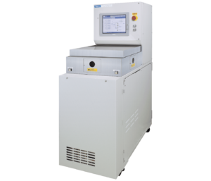
Released compact PECVD system PD-220
Jul.
Acquired field support business from Samco Engineering Co., Ltd.
Jan.
Opened Cambridge Research Laboratory at University of Cambridge, UK
May
Became publicly listed in JSDA Over-the-Counter Trading Securities Market
Jul.
Opened Taiwan Office
Jul.
Opened Production Center I in Kyoto
Nov.
Released production type PECVD system PD-220LC
Dec.
Introduced high speed silicon deep etching technology from Robert Bosch GmbH
Nov.
Opened Shanghai Office
Dec.
Changed company name to Samco Inc.
Dec.
Withdrew from JSDA Over-the-Counter Trading Securites Market and became publicly listed in JASDAQ Securities Exchange Market
May
Released plasma CVD system PD-2203L (Cluster Lab) for general purpose
Sep.
Provided to British business the technology of mass-producing ferroelectric-carbon nanotubes which was developed together with University of Cambridge
Dec.
Released compact batch-type plasma cleaning system PC-300 for cleaning electronic substrate
May
Opened Product Service Center
May
Released dry etching system RIE-800iPB for MEMS
Sep.
Signed a collaborative research agreement with Tsinghua University (China)
Nov.
Released ICP etching system RIE-140iP for LD
Mar.
Opened R&D Center II in Kyoto
May
Released production type MOCVD system MCV-2018 for GaN film deposition
Oct.
Established a subsidiary, Samco Global Service Inc., in Taiwan for field support
Nov.
Released production type ICP etching system RIE-330iPC for LED
Jan.
Started running of Samco Global Service Inc.
Apr.
Held 30th anniversary event at Kyoto Hotel Okura
Oct.
Released R&D type dry etching system RIE-400iPB for MEMS
Apr.
Became listed in Osaka Securies Exchange JASDAQ Market (now TSE JASDAQ (standard) market) as a result of the merge of Osaka Securities of Exchange, Co., Ltd. and Jasdaq Securities Exchange, Inc.
Jul.
Released production type plasma CVD system PD-330STC for TSV
Jul.
Released production type plasma CVD system PD-5400 for LED
Aug.
Opened East Coast Office in North Carolina, U.S. (Relocated to New York in May 2014)
Sep.
Opened Beijing Office
Dec.
Released production type ICP etching system RIE-331iPC for LED
Nov.
Released ICP etching system RIE-600iP for SiC power device
Jul.
Transferred Samco’s stock listing to Tokyo Stock Exchange Market Second Section
Oct.
Released production type ICP etching system RIE-600iPC for SiC power device
Nov.
Released production type RIE system RIE-800iPBC for MEMS
Jan.
Transferred Samco’s stock listing to Tokyo Stock Exchange Market First Section
Mar.
Signed distribution agreement of MOCVD systems with Valence Process Equipment Inc. (U.S.)
May
Acquired UCP Processing (Lichtenstein) as a subsidiary (Later renamed as samco-ucp AG)
Sep.
Increased capital to JPY 1.66 billion through public offering
Dec.
Signed distribution agreement of SiC epitaxial CVD system with Epiluvac AB (Sweden)
Dec.
Released ALD system AL-1 for electronic devices
Jun.
Opened Production Center II in Kyoto
Aug.
Opened Malaysia Office
Sep.
Released Aqua Plasma™ cleaner AQ-2000
Dec.
Released compact ICP etching system RIE-200iPN
Sep.
Held 40th anniversary event at Kyoto Hotel Okura
Jul.
Opened PECVD and ALD demonstration facility in the Production Building II
Dec.
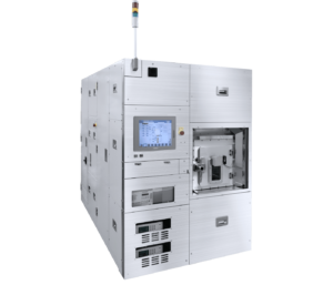
Released cluster tool system Cluster H™ for compound semiconductor device
Mar.
Developed plasma techniques for inactivation of coronaviruses
Mar.
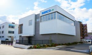
Opened research center for nano thin films & materials
Apr.
Transferred Samco’s stock listing to Prime Market of the Tokyo Stock Exchange
Oct.
Released plasma enhanced ALD system AD-800LP
Oct.
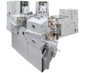
Released three-chamber plasma enhanced CVD system PD-2203LC
Nov.
Started research collaboration with Eastern Switzerland University of Applied Sciences (OST)
Nov.
Decided to construct third R&D facility for innovative semiconductor process equipment
May
Started to construct third R&D facility; Advanced Technology Development Center