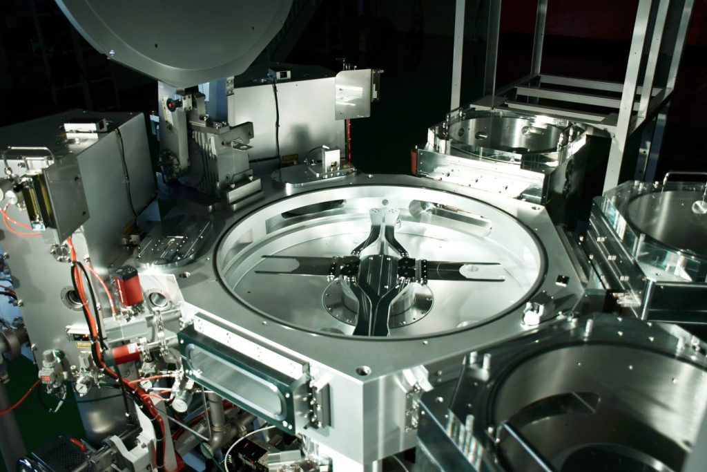
Samco’s etching processes are renowned for their precision and versatility. We offer Atomic Layer Etching (ALE), Inductively Coupled Plasma (ICP) Etching, Deep Reactive Ion Etching (DRIE), Reactive Ion Etching (RIE), and Xenon Difluoride Etching. Our expertise spans a variety of materials, including GaN, GaAs, InP, Si, SiO₂, and SiC, making us a trusted partner for compound semiconductor applications, MEMS, RF filters, and more.
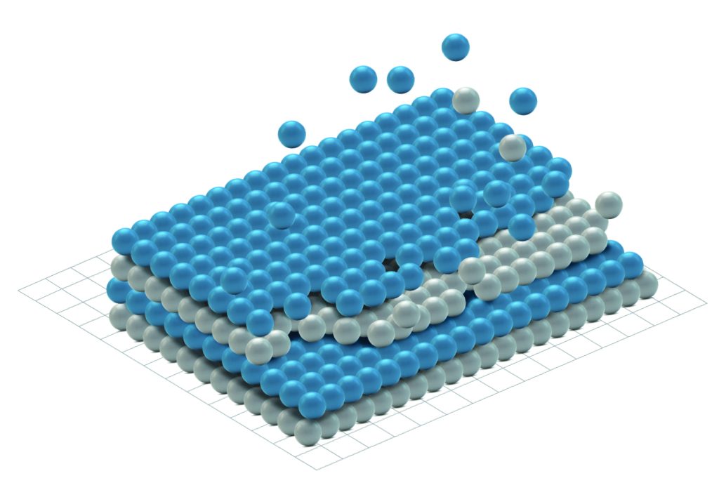
Atomic Layer Etching (ALE) is a technology that separates the adsorption and reaction steps in the etching process and repeats each step to control etching depth at the nano-level. ALE is gaining increasing attention as semiconductor devices become finer, emerging as a key process in the development of next-generation devices. ALE is expected to find applications in processes such as controlling GaN or AlGaN film thickness and maintaining surface smoothness through low-rate etching, as well as in p-GaN/AlGaN high selectivity etching of GaN HEMT devices.
Samco offers high precision and high speed processing of III-V compound semiconductors such as GaN, GaAs, InP and quaternary materials.
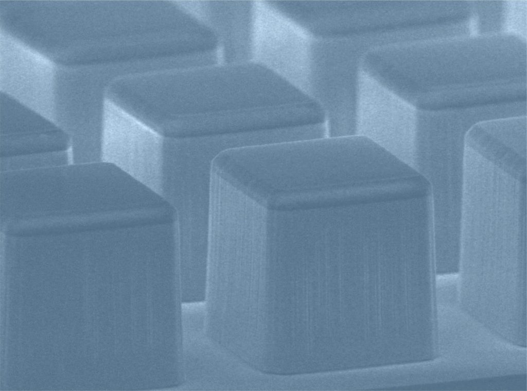
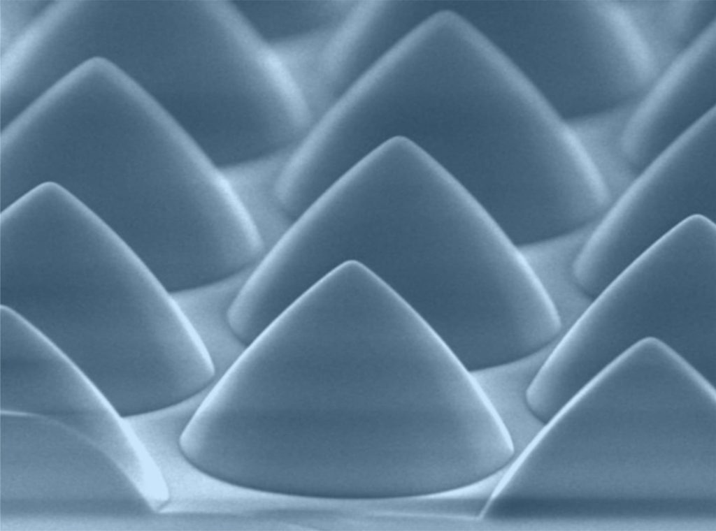
Samco was the first of Japan’s semiconductor process equipment manufacturers to obtain a Bosch Process license. By harnessing the Bosch Process, Samco’s Si DRIE systems have proven effective in deep, vertical, high-speed Si deep etching for both R&D and production. Also, Samco developed high precision processing at the nano level using ICP etching and RIE systems.
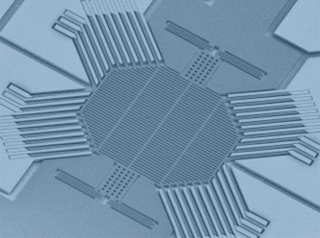
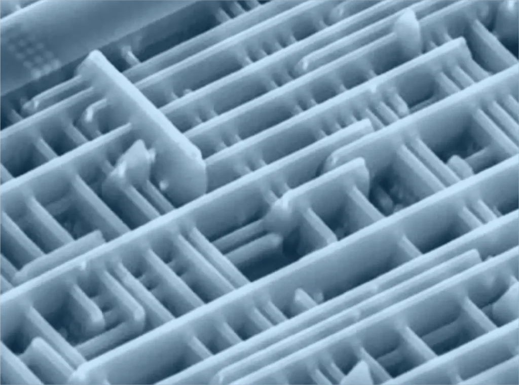
Samco has extensive experience in selectively removing both dielectric (insulating) and metallic (conductive) materials. These processes include the use of many types of materials to produce smaller, more complex, and narrower features. These etching processes help to manufacture the RF filters (both SAW and BAW devices) and capacitors.
Samco provides advanced solutions tailored for IC failure analysis to enhance device reliability and pinpoint failure modes. Leveraging decades of dry etching expertise, Samco’s systems are used globally in both production and failure analysis (FA) labs, offering precise etching that meets the stringent demands of modern semiconductor manufacturing.