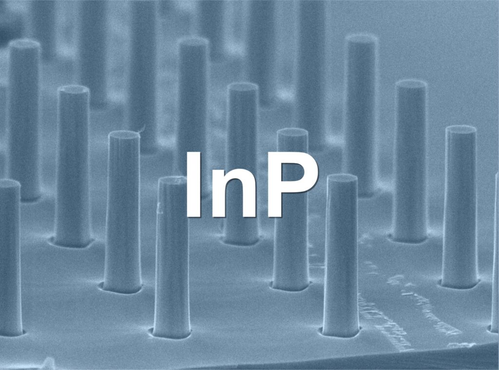

Indium Phosphide (InP) is a key III–V semiconductor used in high-speed photonics, telecommunications, infrared devices, and advanced RF applications. Because InP forms non-volatile etch byproducts, controlling sidewall angles and suppressing polymer redeposition are critical challenges in plasma dry etching.
Samco provides advanced ICP-RIE etching solutions engineered to achieve vertical profiles, smooth surfaces, and highly accurate dimensional control for InP-based devices. With decades of III–V process expertise, our systems deliver reliable results for both R&D and volume manufacturing.
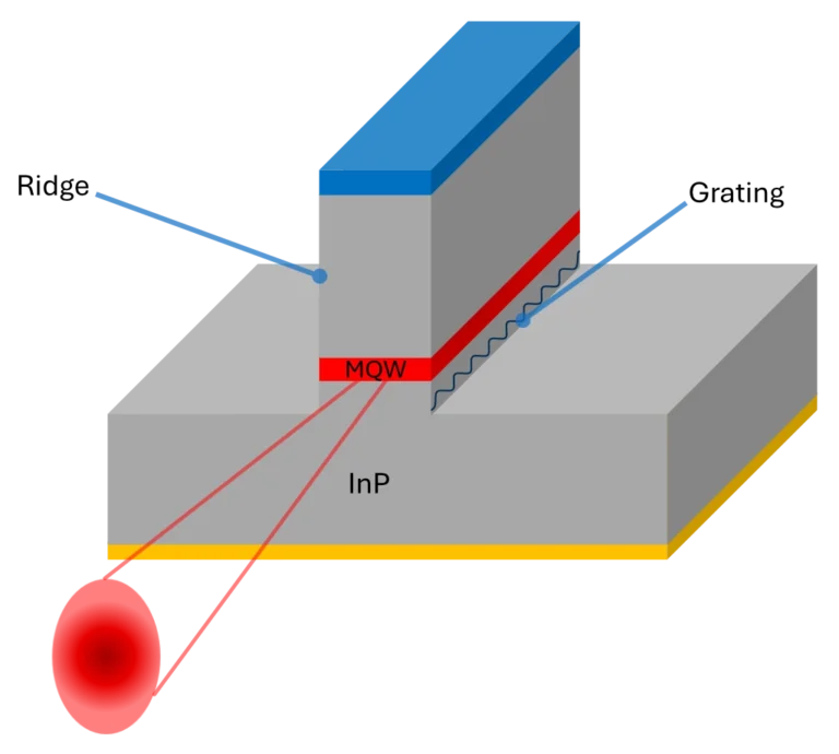
Samco provides etching, deposition, and surface-processing systems for InP-based device fabrication, supporting ø3-inch, ø4-inch, and ø6-inch wafer processes. Our lineup includes ICP-RIE, CCP-RIE, PECVD, and ALD systems for applications such as grating, ridge, lens, photonic crystal, and advanced InP device structures.
InP is distinguished by its excellent electrical and optical properties:
These characteristics make InP the foundation of:
Because many InP-based structures require vertical pillars, gratings, ridges, or deep waveguide features, high-quality anisotropic plasma etching is essential.
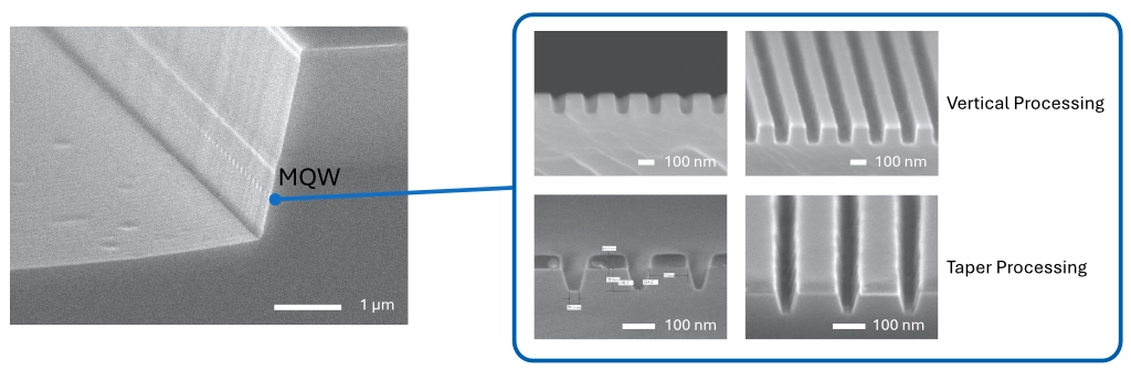
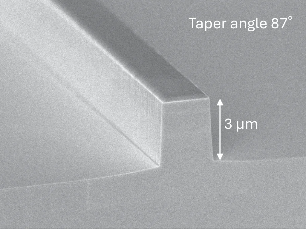
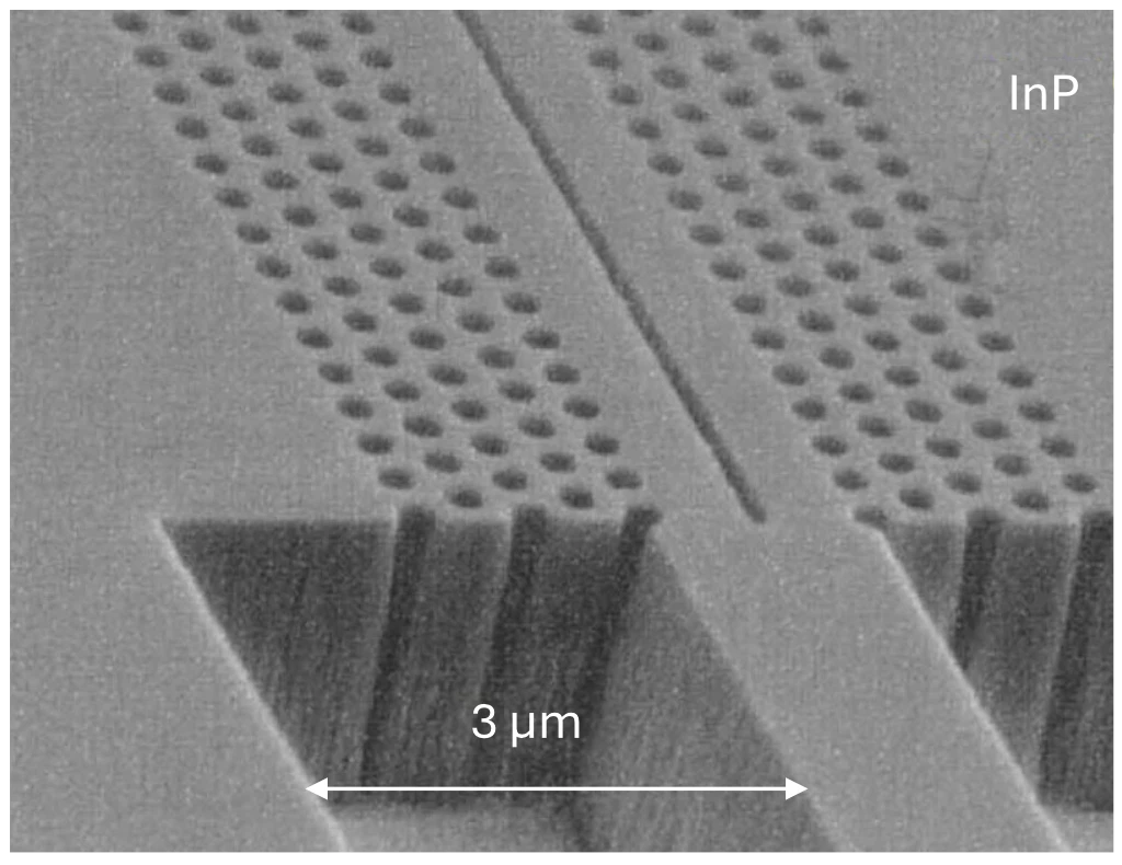
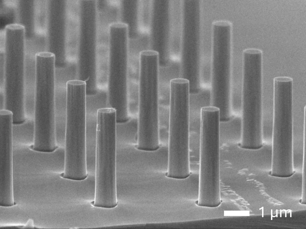
InP etching often suffers from rounded or tapered sidewalls due to non-volatile etch residues. Samco’s optimized ICP configurations minimize polymer deposition and enable highly anisotropic etching for pillars, waveguides, gratings, and resonator structures.
Samco’s ICP-RIE technology is optimized to address the unique challenges of InP etching:
These capabilities support applications ranging from laser diode ridge formation to nanopillar arrays and photonic crystals.
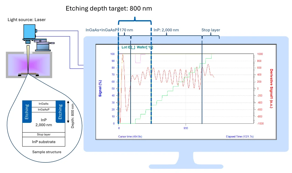
Endpoint detection via peak counting enabled by selecting an appropriate light source.
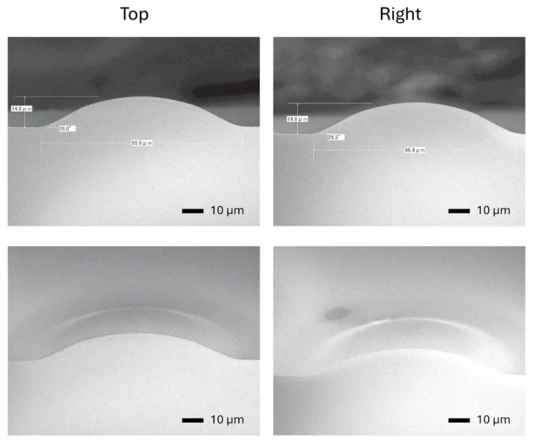
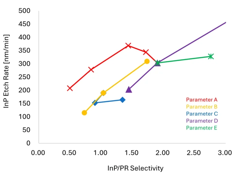
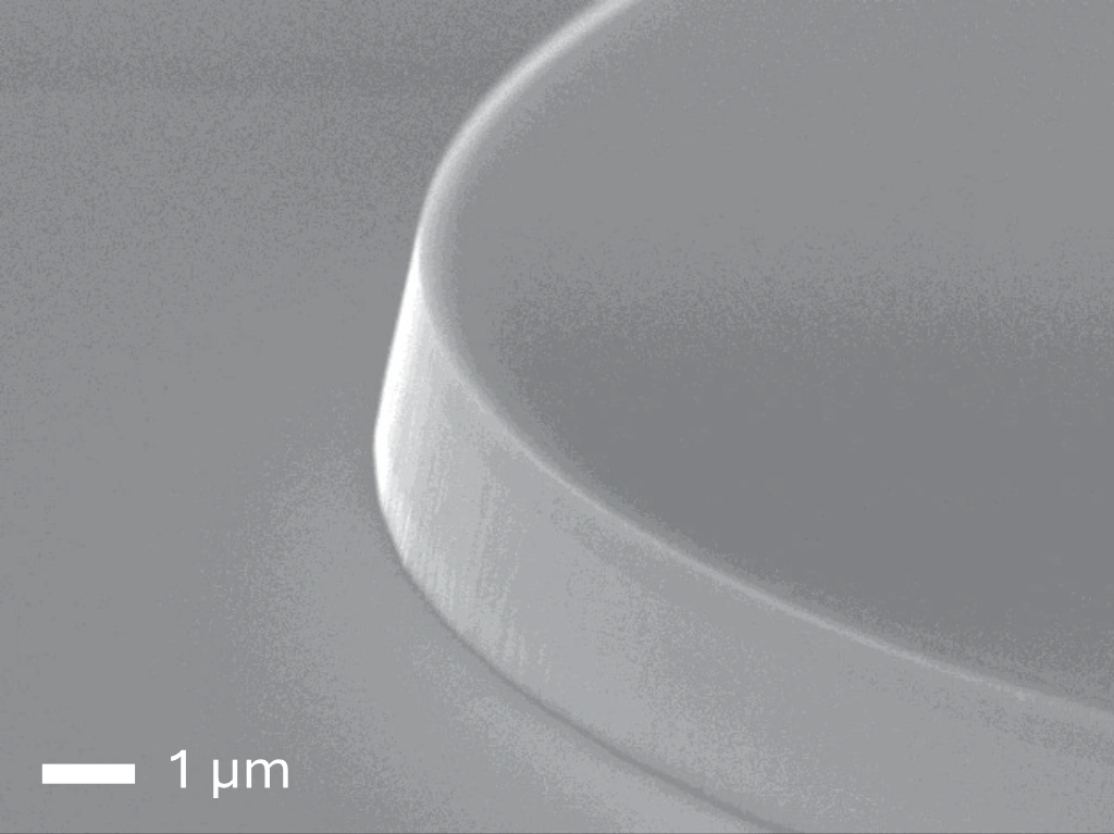
Optimized process parameters ensure highly reproducible control of InP/PR selectivity and InP etch rate, enabling stable realization of customized lens profiles.
InP etching often suffers from rounded or tapered sidewalls due to non-volatile etch residues. Samco’s optimized ICP configurations minimize polymer deposition and enable highly anisotropic etching for pillars, waveguides, gratings, and resonator structures.
Controlling surface roughness (RMS) is critical for high-performance LDs and photonic crystals. Samco’s process conditions maintain smooth surfaces on both sidewalls and trench bottoms, improving optical confinement and reducing propagation losses.
Our InP etch processes deliver:
These benefits support both fabrication flexibility and high device yield.
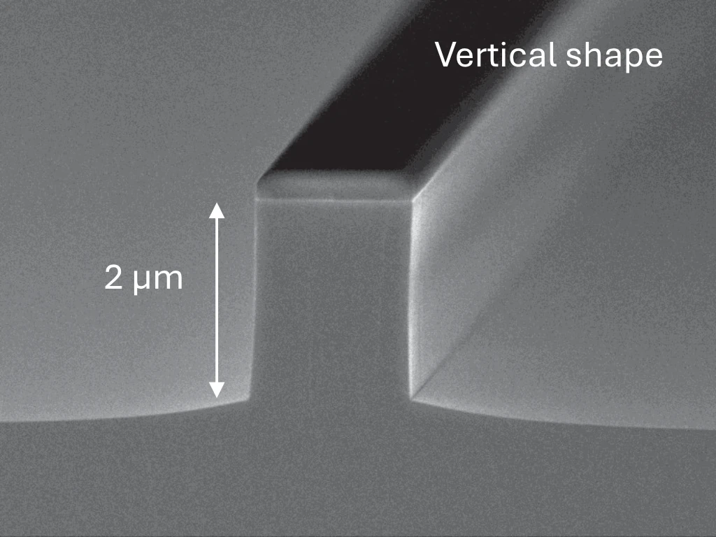
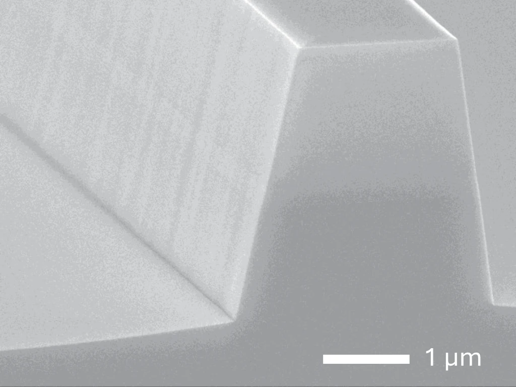
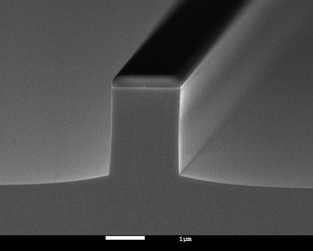
The anisotropic and small footing ridge shape with a width of 1.8 μm and a depth of 2.5 μm has been achieved.
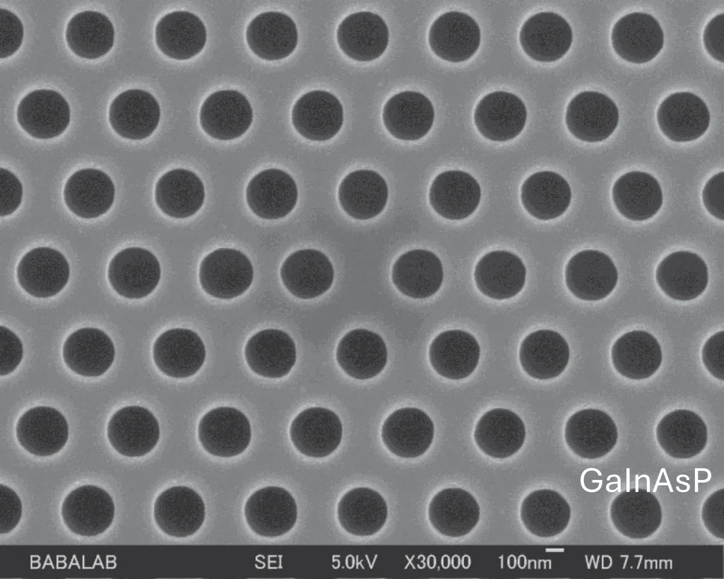
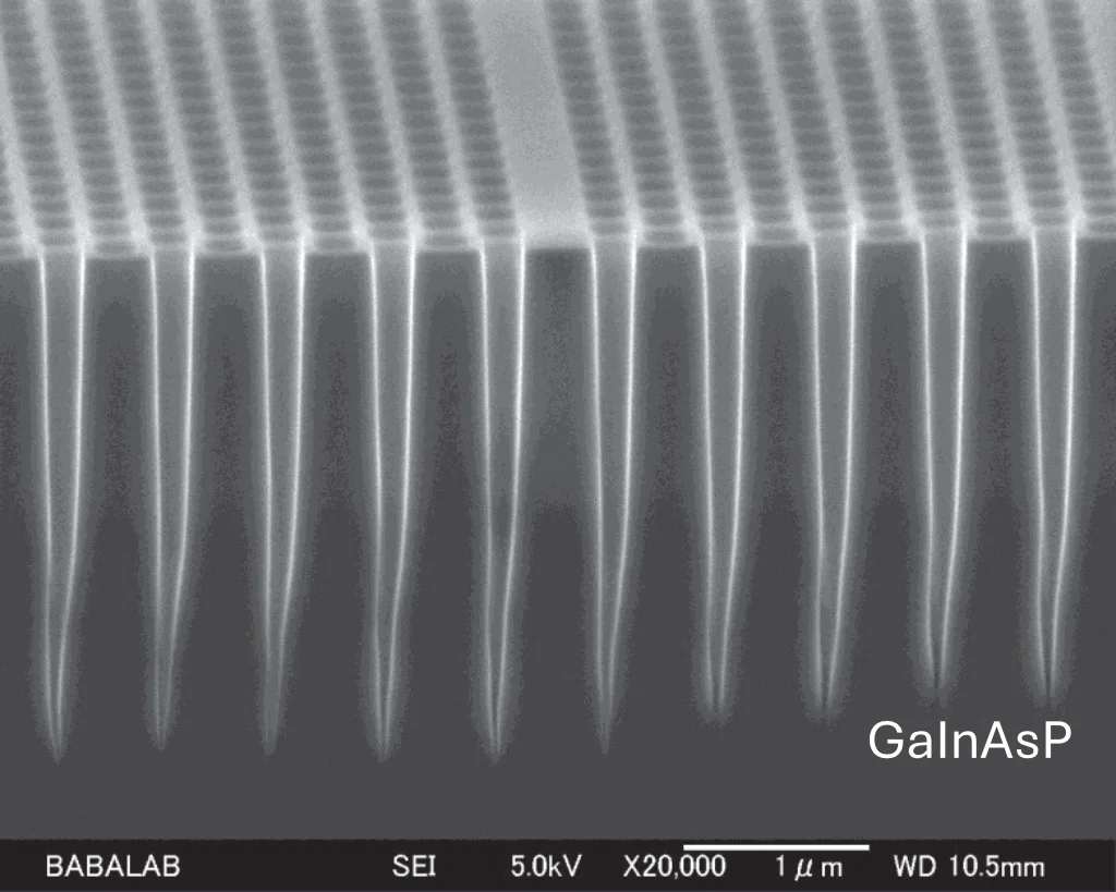
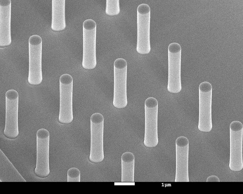
This process can be applied to semiconductor lasers and photonic crystals. A smooth pillar, 0.7 µm in diameter and 4 µm deep, with vertical, no sidewall or bottom roughness, has been formed.