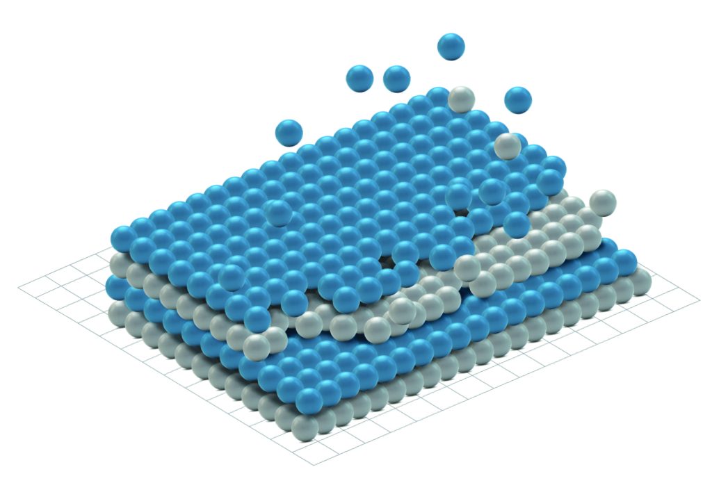
Atomic Layer Etching (ALE) is a technology that separates the adsorption and reaction steps in the etching process and repeats each step to control etching depth at the nano-level. ALE is gaining increasing attention as semiconductor devices become finer, emerging as a key process in the development of next-generation devices. ALE is expected to find applications in processes such as controlling GaN or AlGaN film thickness and maintaining surface smoothness through low-rate etching, as well as in p-GaN/AlGaN high selectivity etching of GaN HEMT devices.
Gallium Nitride (GaN) etching using ALE achieves exceptional precision and surface smoothness, meeting the stringent requirements of advanced GaN-based devices like HEMTs and LEDs and laser diodes. This process ensures high selectivity and minimal damage, maintaining the integrity of GaN’s material properties while enabling tight dimensional control. Ideal for applications demanding low defect densities and uniformity, Samco’s GaN ALE solutions support cutting-edge advancements in power electronics, optoelectronics, and RF technologies.
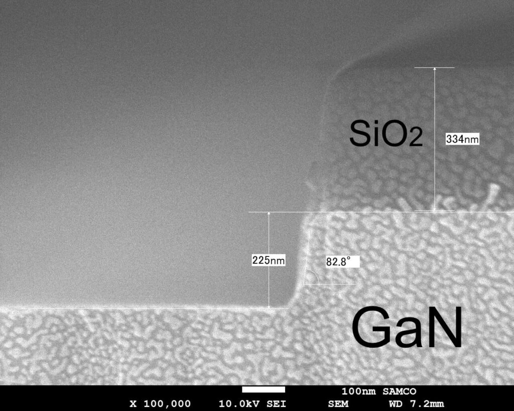
GaN was etched using ALE with a SiO₂ mask, achieving a trench width of 0.7 µm and an etching depth of 225 nm at 7.0 Å/cycle. With excellent controllability, this process supports nanopatterning applications like photonic crystals and recess etching for GaN HEMTs.
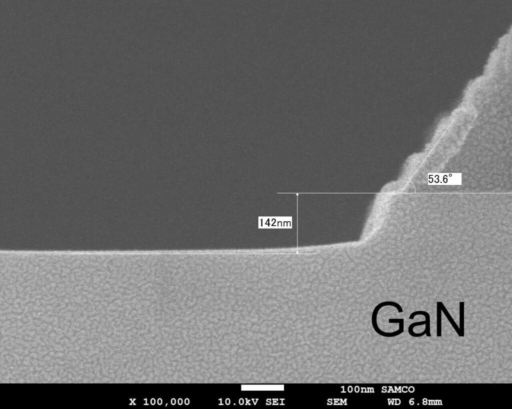
Using ALE with a photoresist mask, GaN was etched at 9.5 Å/cycle to a depth of 142 nm with a trench width of 5 µm, demonstrating excellent process controllability. This method is suitable for nanopatterning applications like photonic crystals and GaN HEMT recess etching.
Atomic Layer Etching (ALE) of silicon enables precise material removal with unparalleled surface smoothness and dimensional accuracy. This controlled process is ideal for applications requiring atomic-level precision, such as advanced semiconductor devices, MEMS, and photonic components. With its potential for low-damage etching and high selectivity, ALE of silicon opens pathways for innovations in next-generation microelectronics and nanoscale devices.
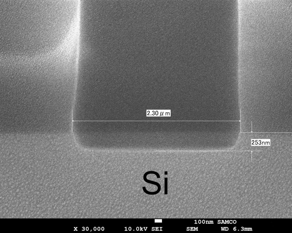
Si was etched via ALE with a photoresist mask to a depth of 253 nm at 12.5 Å/cycle, achieving uniform etching across hole diameters of 2 µm, 20 µm, and 50 µm, with no micro-loading effect. (SEM photograph shows the results for hole diameter 2um.)
ALE of silicon dioxide delivers high precision and surface quality, meeting the demands of intricate patterning and structural control. This process is particularly valuable for applications in microfabrication, dielectric layer processing, and advanced integrated circuit designs. By offering uniformity and selectivity, ALE of SiO₂ is poised to drive progress in fields requiring high-resolution and low-damage processing of dielectric materials.
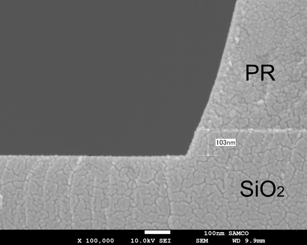
SiO₂ was etched via ALE with a photoresist mask to a depth of 103 nm at 8.5 Å/cycle, offering high selectivity for SiO₂/SiN etching in Self-Aligned Contact applications.