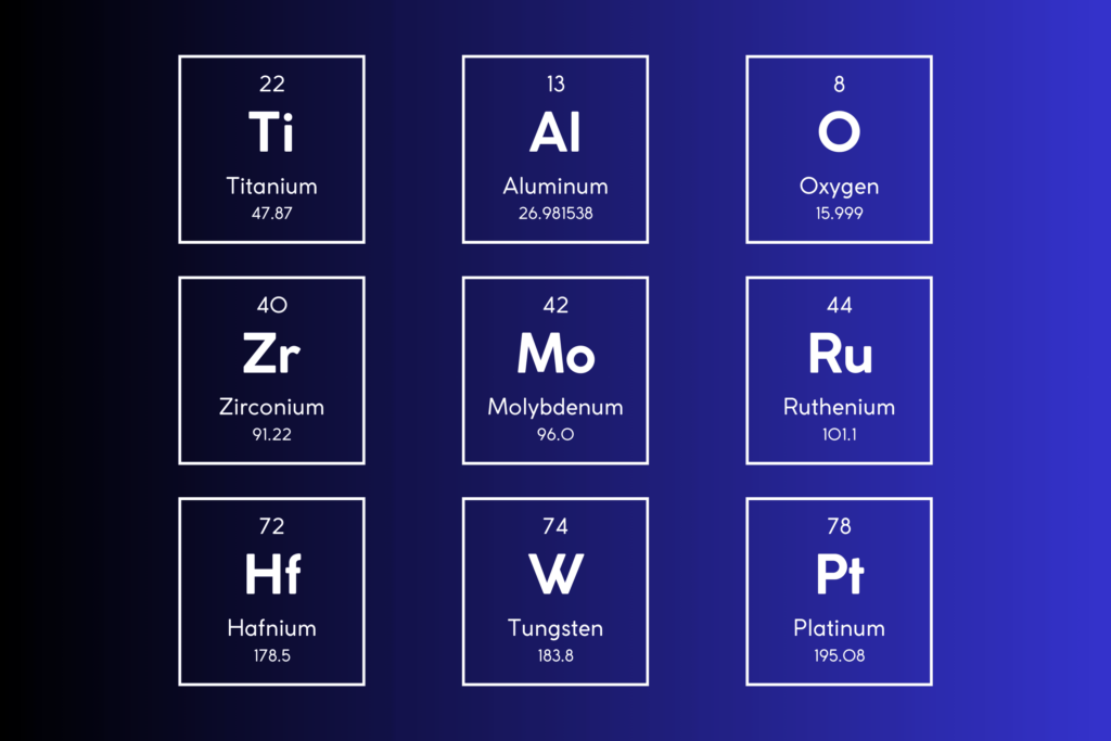

Samco has extensive experience in selectively removing both dielectric (insulating) and metallic (conductive) materials. These processes include the use of many types of materials to produce smaller, more complex, and narrower features. These etching processes help to manufacture the RF filters (both SAW and BAW devices) and capacitors.
Samco shows strong presence in GaN plasma etching for various applications such as laser diodes and LEDs.
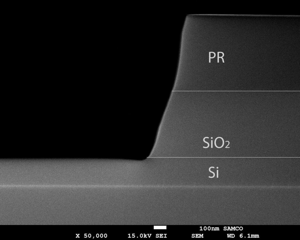
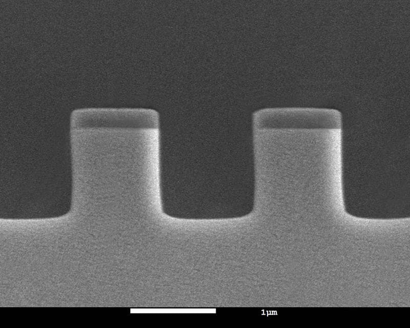
The SiO₂ trench etching process achieves precise sidewall angle control while maintaining the resist profile. Etching uniformity of ±1% is achieved across ø6″ Si wafers.
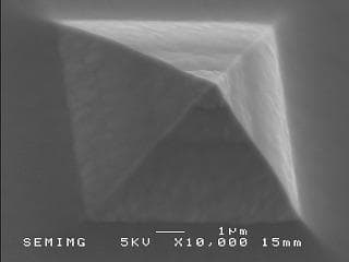
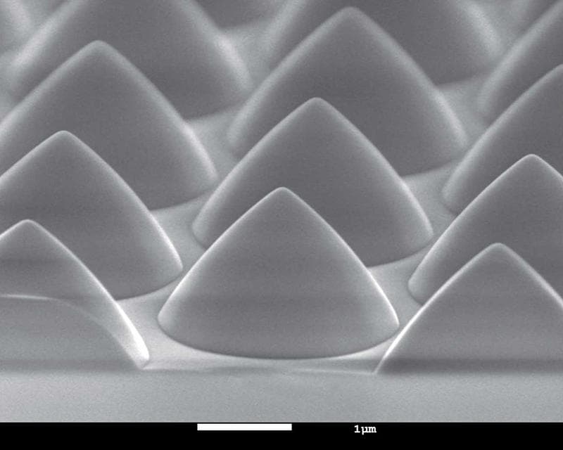
Three-dimensional quartz glass fabrication using a thick film resist and grayscale exposure to create a 10 µm square pyramid structure, with selectivity around 1.
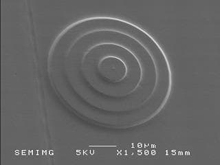
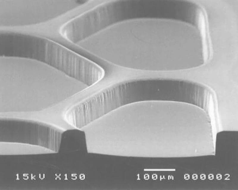
Three-dimensional quartz glass fabrication using a thick film resist and grayscale exposure to form a ø50 µm stepped structure, with selectivity around 1.
Microfabrication of quartz glass for imprint molds, achieving 5 µm line-and-space patterns with the RIE-400iPB. Selectivity to the Cr mask is 100:1 with a 6 µm depth and forward taper.
Anisotropic plasma etching of SiO₂ using the large-area RIE plasma etching system RIE-300NR, enabling batch processing of multiple wafers with excellent uniformity.
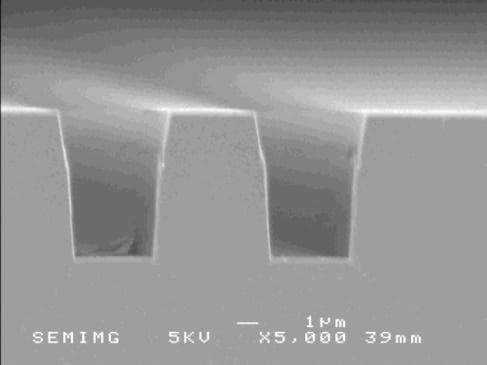
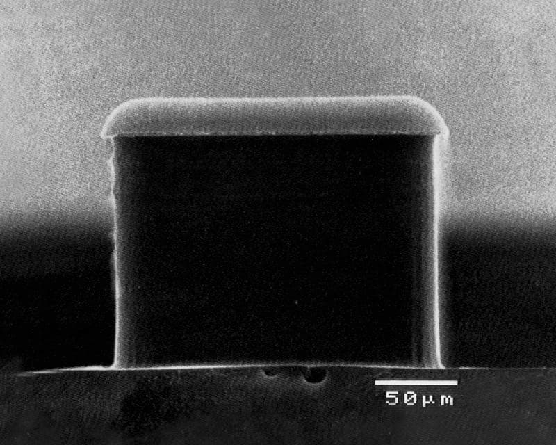
Precise anisotropic processing with 50 µm width and 27.3 µm depth using a Cr mask, with an etch rate of 1 μm/min.
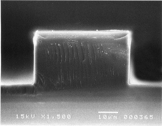
Deep etching of quartz to 150 μm using a Ni mask, achieving an etch rate of 400 nm/min.
Samco’s advanced GaAs etching technology ensures superior uniformity across 6-inch wafers, supporting precise device production. Our optional interferometry endpoint detection system guarantees stable and accurate etch stops, even across multiple wafers. The market for Vertical Cavity Surface Emitting Lasers (VCSELs), which utilize GaAs mesa etching, is rapidly expanding. These lasers are integral to various applications, including smartphones and autonomous driving systems. Samco’s GaAs etching solutions are engineered to meet the high demands of these emerging technologies.
PSS processing creates a cone pattern (~2.5 μm diameter) on sapphire, reducing GaN crystal defects and enhancing LED brightness through improved internal reflection.
High-speed processing has achieved an 85 μm deep etch with strong anisotropy, resulting in angles of 80-90°.