language
Samco Inc.
USA Website Next Gen
Inductively Coupled Plasma (ICP) Etching Systems
You are here:
- Home
- Products
- Etching Systems
- Inductively Coupled Plasma (ICP) Etching…
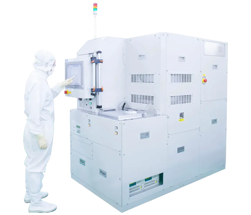
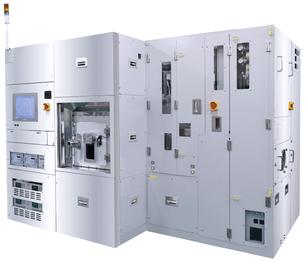
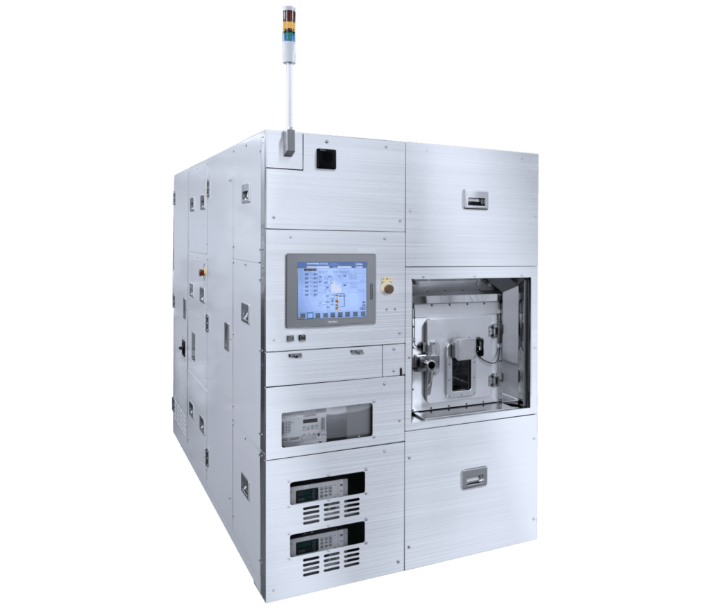
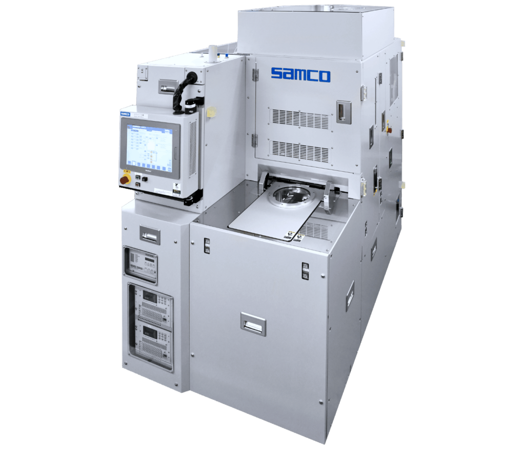
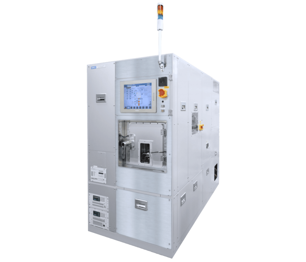
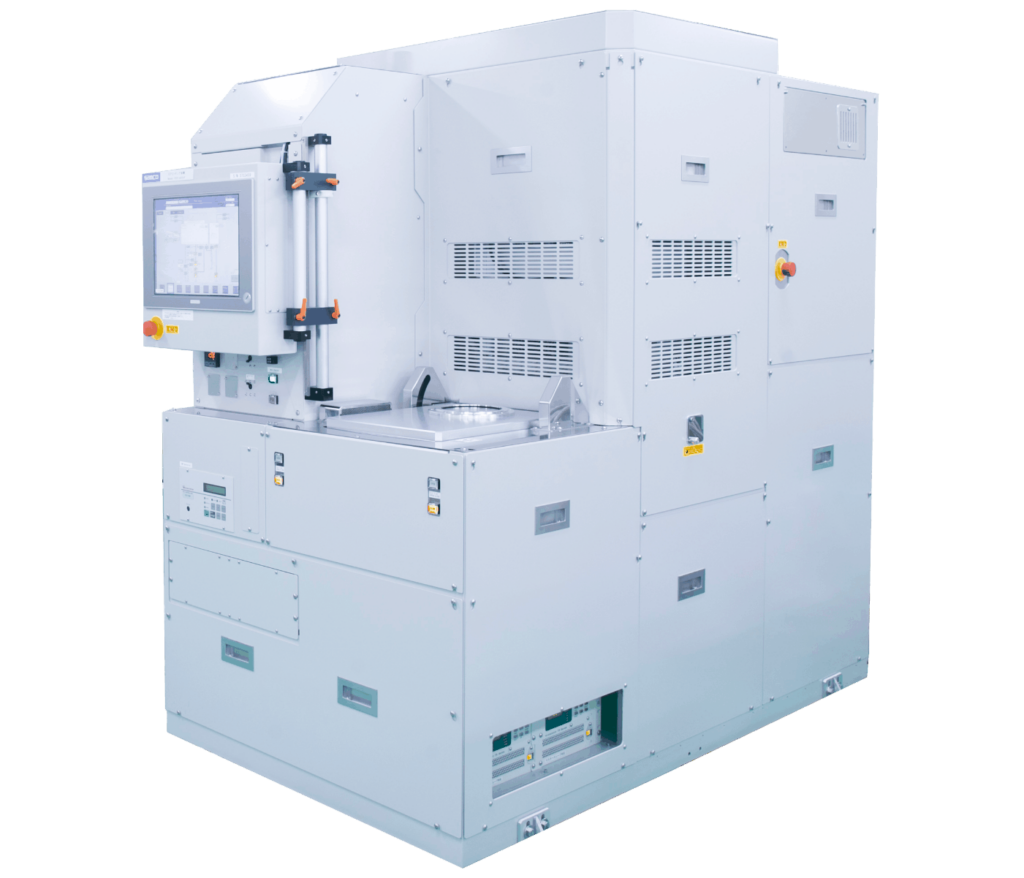
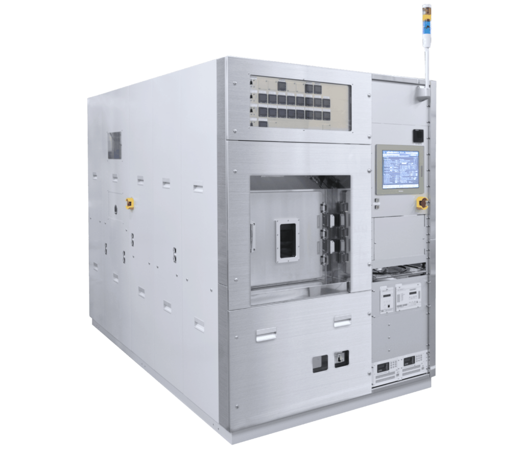
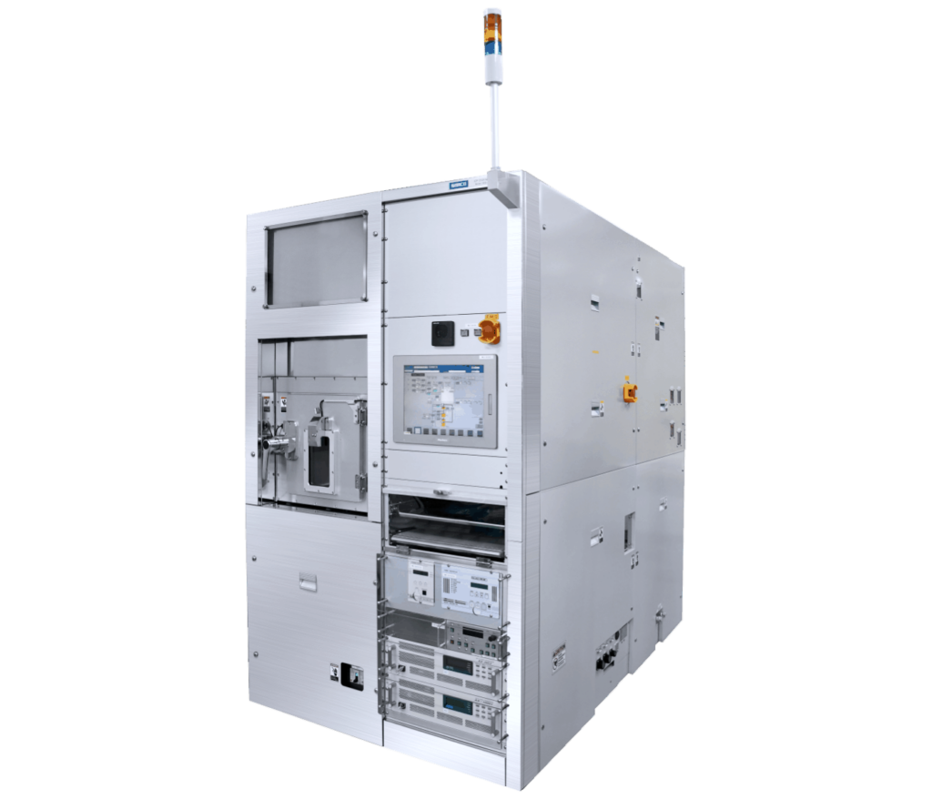
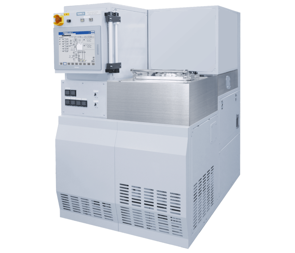
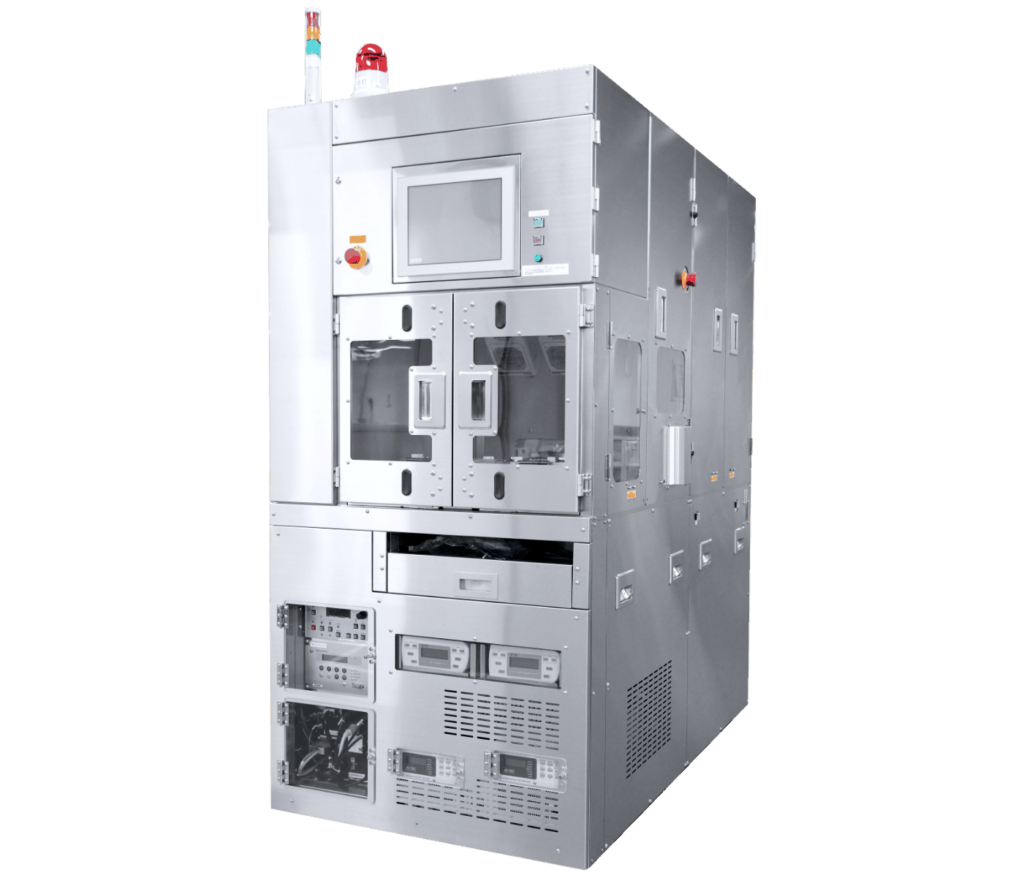
Samco’s Inductively Coupled Plasma (ICP) etching systems deliver high-density plasma solutions tailored to meet the unique process requirements of both research and production environments. Designed for reliability and durability, our compact systems enable precise etching across a wide range of materials, including III-V compound semiconductors (GaN, GaAs, InP), silicon, SiC, quartz, glass, dielectrics, and metals.
Samco’s inductively coupled plasma (ICP) etching systems provide advanced plasma etching solutions for cutting-edge technologies that drive the future, including:
The precise fabrication of these devices relies on highly accurate dry plasma etching processes, especially for compound semiconductor materials. Samco’s ICP etching systems, equipped with the patented Tornado ICP™ coil, achieve plasma densities up to 1,000 times higher than conventional capacitive coupled plasma reactive ion etching (CCP-RIE) systems. This innovation ensures exceptional plasma uniformity, enabling high-speed, high-aspect-ratio etching for compound semiconductors, silicon, and metal thin films.
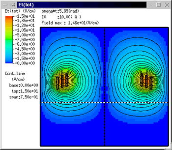
(a) Contour Line of Electric Field by Tornado ICP™
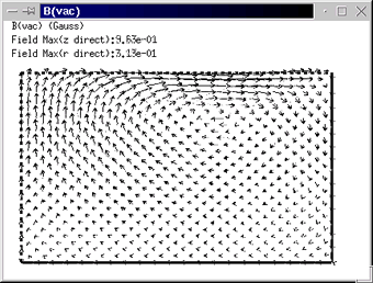
(b) Magnetic Field by Tornado ICP™
By leveraging advanced electromagnetic field simulations, Samco has optimized the Tornado ICP™ coil for outstanding etching performance, making our systems a trusted choice for research and production in industries spanning semiconductors, optoelectronics, and beyond.