Samco’s advanced systems are designed to address the diverse needs of various markets, delivering precision and reliability across a range of applications. Our solutions are pivotal in MEMS device fabrication, including deep silicon etching and free-standing structure release. For laser diodes, our proprietary technologies enhance compound semiconductor processing from epi growth to reflective layer formation. In the realm of high-brightness LEDs, we support key manufacturing steps such as patterned sapphire substrate fabrication and device isolation. Our TSV processing technologies improve 3D IC integration, while our SAW device solutions and RF device process solutions cater to high-performance applications in telecommunications and defense. Each system is engineered to meet the rigorous demands of these sectors, ensuring high-quality and efficient production.
Samco DRIE systems provide reproducible process solutions of deep silicon etching. Also, PECVD systems and XeF₂ etching systems are available for both R&D and production.
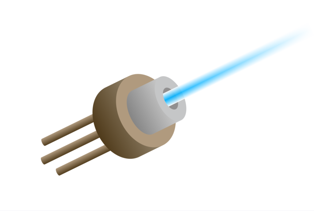
Laser diode fabrication with compound semiconductors is one of Samco’s proprietary fields.
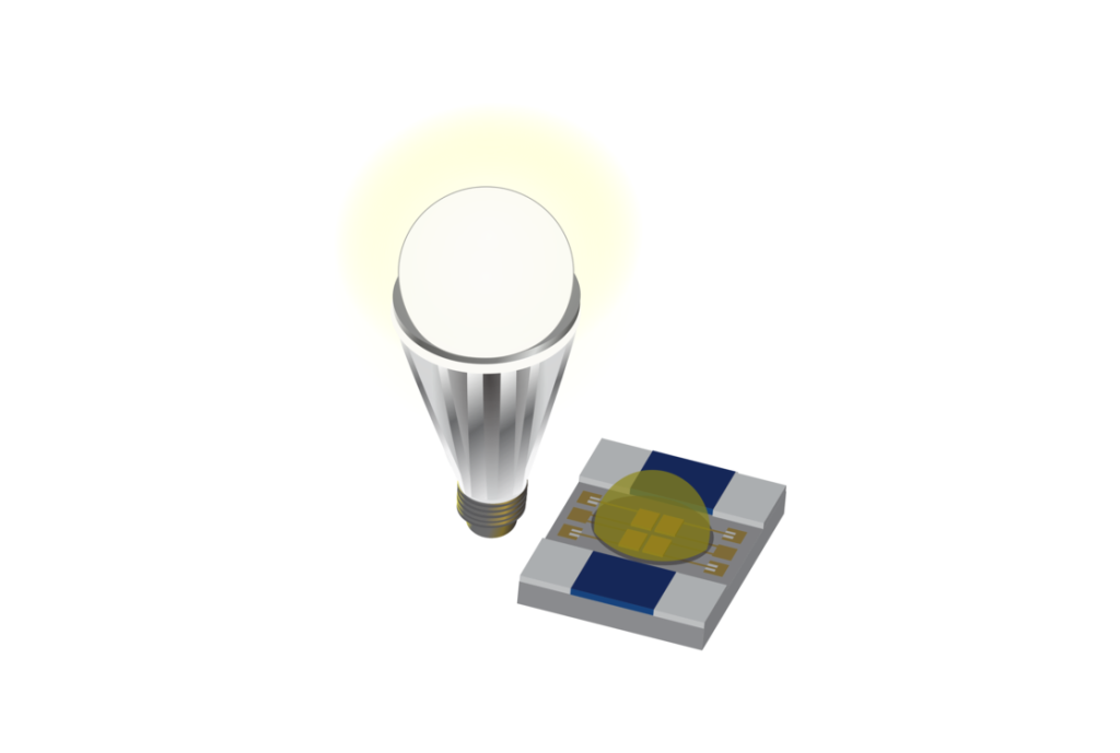
Samco has provided process solutions including Patterned Sapphire Substrate (PSS) fabrication to major HB LED manufacturers. Both single and batch wafer processing are available.
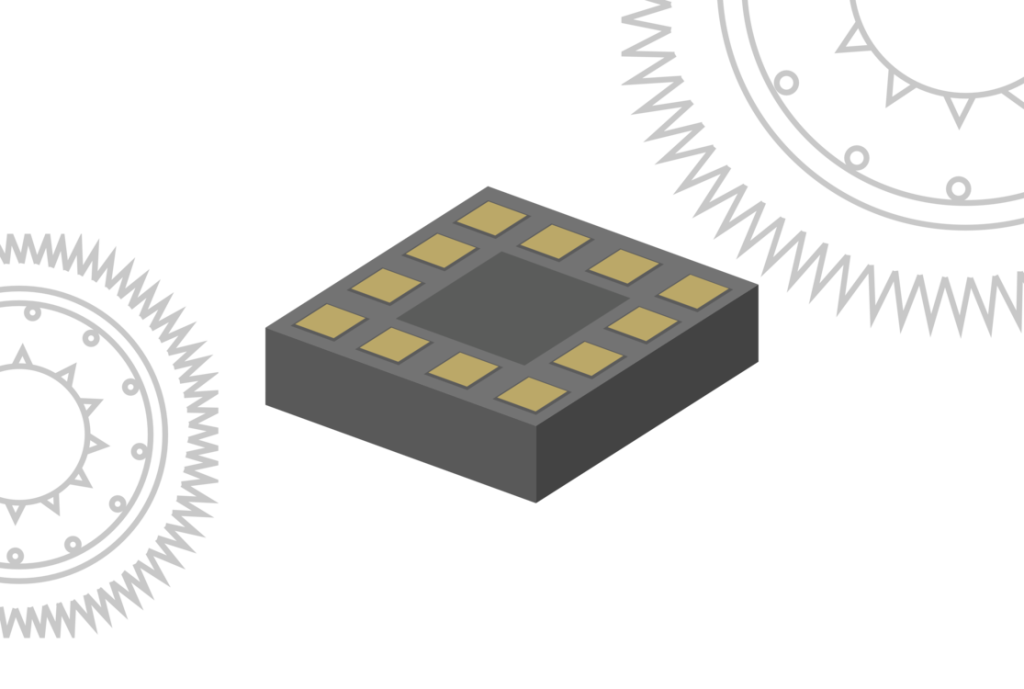
TSV fabricated with Samco deep silicon etching and cathode low-temperature PECVD technologies will improve device performance.
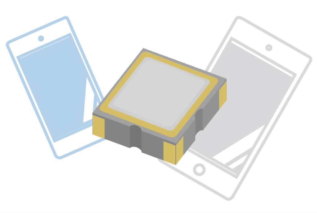
Samco has provided process solutions to major industry-leading SAW/BAW filter manufacturers.
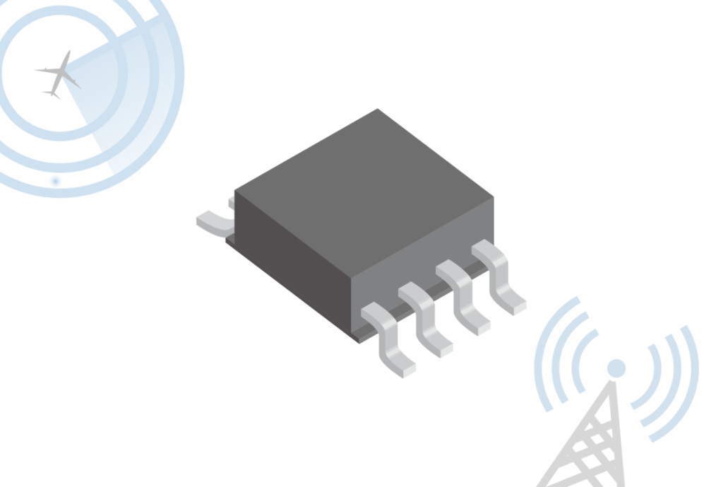
Samco offers process solutions of wide bandgap semiconductors including GaAs, GaN and InP for RF device production in the field of telecommunication and defense applications.