Samco provides advanced solutions tailored for IC failure analysis to enhance device reliability and pinpoint failure modes. Leveraging decades of dry etching expertise, Samco’s systems are used globally in both production and failure analysis (FA) labs, offering precise etching that meets the stringent demands of modern semiconductor manufacturing.
Our layer removal processes allow the exposure of up to 5 metal layers without risking delamination or erosion, ensuring dependable and repeatable results. With options ranging from die to 300 mm wafer processing, Samco’s systems are equipped with cutting-edge features like endpoint detection for precise, reproducible etch stops.
Our plasma etching process enables high-selectivity, high-aspect ratio etching across a diverse range of materials, facilitating targeted passivation removal, defect decoration, and layer-by-layer inspection for accurate failure analysis.
Using advanced plasma etching technology, Samco’s systems are compatible with the following materials:
Silicon (Si)
Oxides
Nitride
Inter Metal Dielectrics (IMD)
Inter Layer Dielectrics (ILD)
Low-k Dielectrics
Polymers
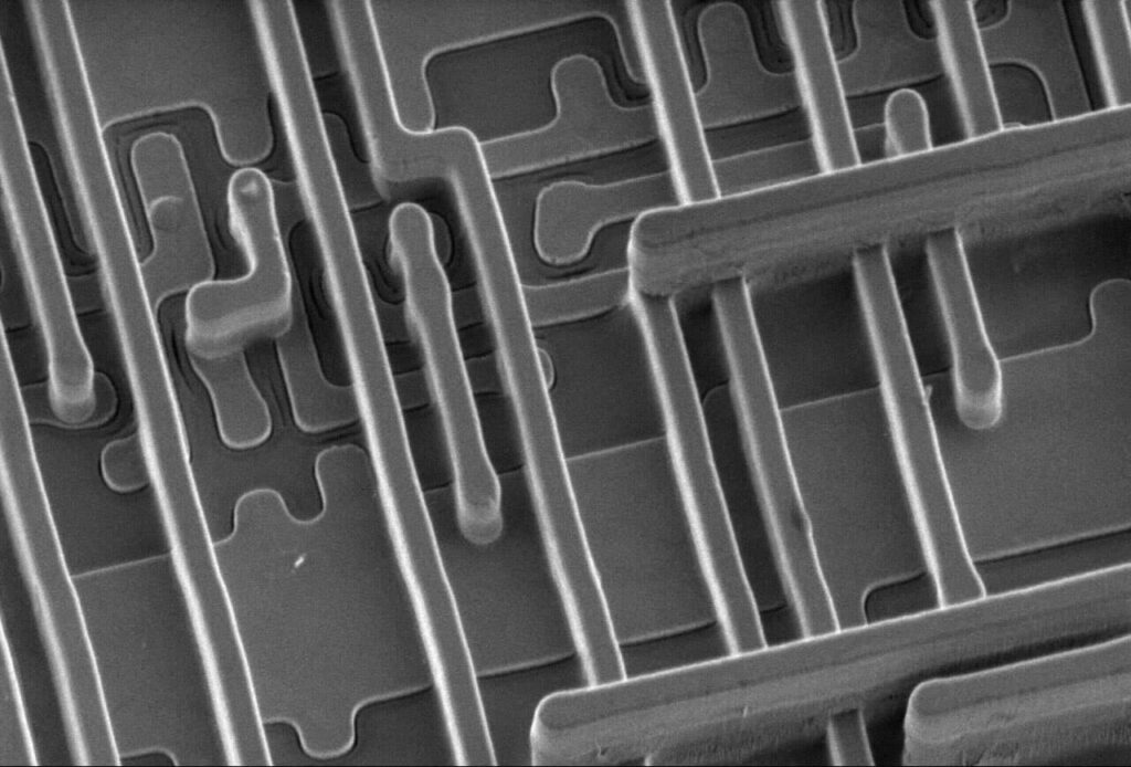
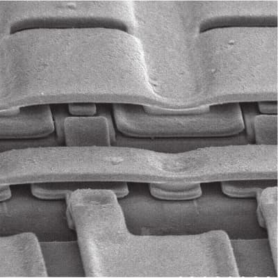
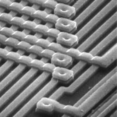
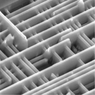
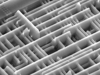
Reliable removal of up to 5 layers without compromising the integrity of underlying Al or Cu lines enhances inspection accuracy and reliability. This technique enables layer-by-layer depassivation and failure inspection of complex-structured dies.
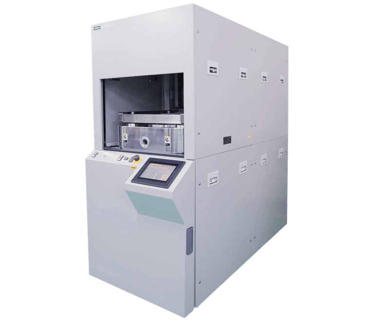
Samco’s plasma etching systems provide a comprehensive lineup from table-top RIE systems for single dies to large-chamber systems for up to 300 mm wafers. With open-load RIE options for low ownership costs and ICP systems for low-bias power processing, we cater to diverse customer needs.
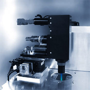
Reliable endpoint detection is essential for consistent, high-quality etching. Samco’s optional endpoint detection system offers automated, precise thickness monitoring for transparent films like oxide and nitride, enabling full process control and repeatability.
Samco’s plasma decapsulation solutions offer unmatched precision and reliability, supporting everything from prototyping to high-volume manufacturing. Trusted globally, our systems provide:
Defect analysis of exposed 5-layer Al wiring using RIE plasma etching system; successfully removing silicon nitride (SiN) passivation layer and silicon oxide (SiO₂) interlayer insulator, preserving the underlying Al wiring.