Markets Overview & Process Solutions
Samco’s advanced systems are designed to address the diverse needs of various markets, delivering precision and reliability across a range of applications. Our solutions are pivotal in MEMS device fabrication, including deep silicon etching and free-standing structure release. For laser diodes, our proprietary technologies enhance compound semiconductor processing from epi growth to reflective layer formation. In the realm of high-brightness LEDs, we support key manufacturing steps such as patterned sapphire substrate fabrication and device isolation. Our TSV processing technologies improve 3D IC integration, while our SAW device solutions and RF device process solutions cater to high-performance applications in telecommunications and defense. Each system is engineered to meet the rigorous demands of these sectors, ensuring high-quality and efficient production.
MEMS Devices
Samco DRIE systems provide reproducible process solutions of deep silicon etching. Also, PECVD systems and XeF₂ etching systems are available for both R&D and production.
- Deep Silicon Etching by the Bosch Process
- Photoresist Ashing
- Surface Cleaning before Packaging
- XeF₂ Etching for Free-standing Structure Release
Laser Diodes
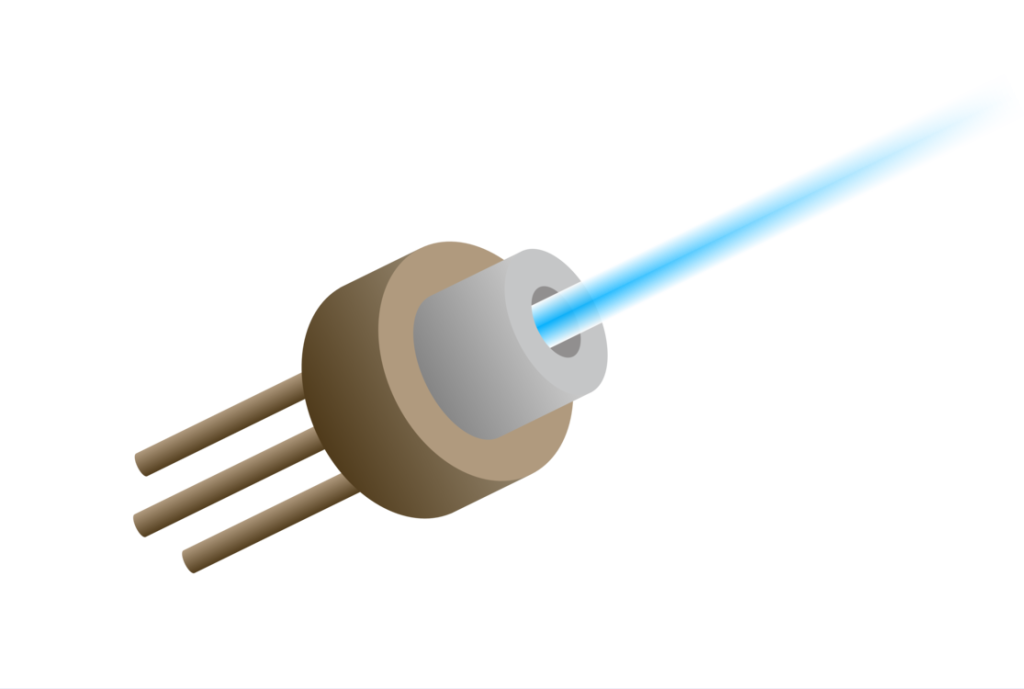
Laser diode fabrication with compound semiconductors is one of Samco’s proprietary fields.
- Ridge Formation by Dry Etching
- Passivation Film Deposition
- Exposure of p-Contact Layer (SiO₂ Etching)
- Reflective Layer Formation by PECVD
High Brightness LEDs
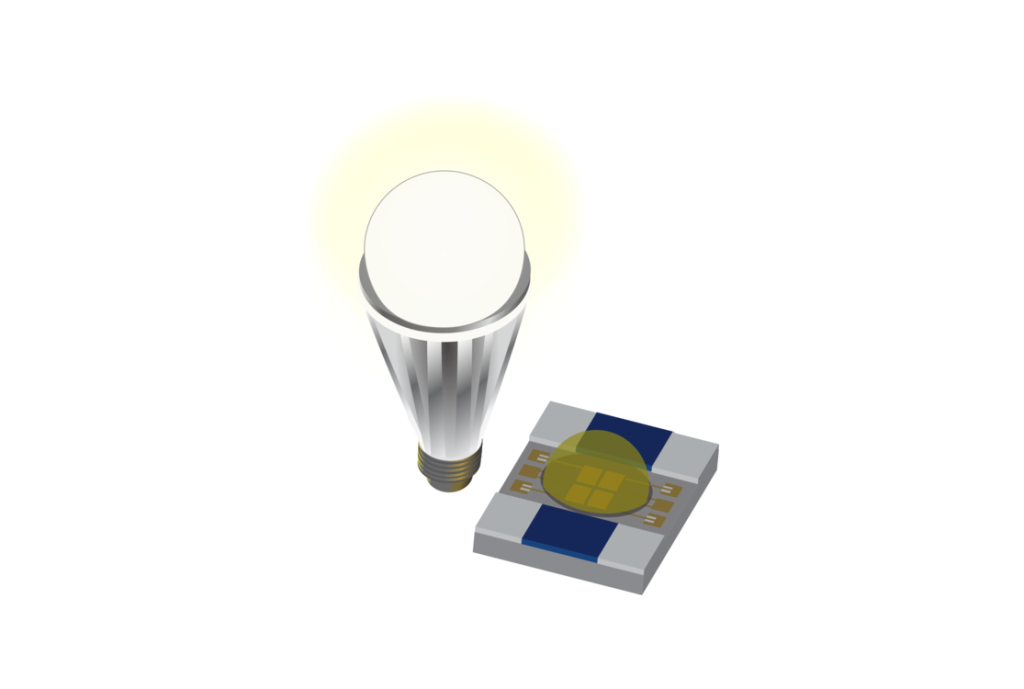
Samco has provided process solutions including Patterned Sapphire Substrate (PSS) fabrication to major HB LED manufacturers. Both single and batch wafer processing are available.
- PSS Fabrication by Sapphire Etching
- p-GaN/Active/n-GaN Layer Deposition by MOCVD
- Expose n-GaN Layer by Dry Etching
- Device Isolation by GaN Etching
- Passivation Deposition by PECVD
- Contact Hole Formation by SiO2 Etching
- Plasma Dicing
TSV Processing for 3D IC Integration
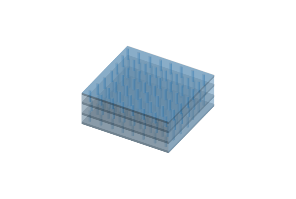
TSV fabricated with Samco deep silicon etching and cathode low-temperature PECVD technologies will improve device performance.
- Via Hole Fabrication using the Bosch Process
- Photoresist Ashing
- Insulation Film Deposition on Via Hole
- Exposure of Lower Electrode by SiO₂ Etching
- Cu Plug Exposure by Dry Etching
- Passivation Film Deposition by PECVD
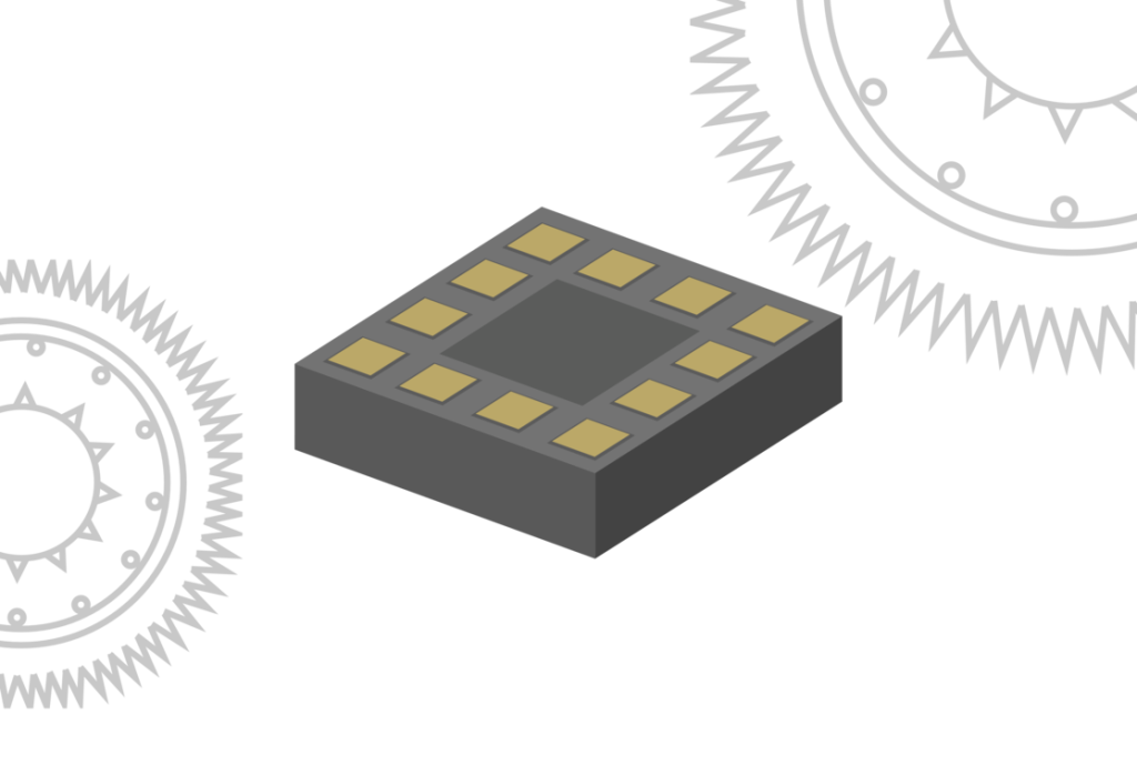
SAW/BAW Filters
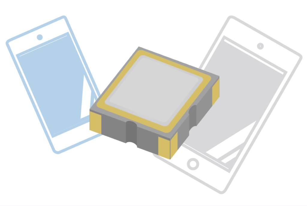
Samco has provided process solutions to major industry-leading SAW/BAW filter manufacturers.
- Photoresist Patterning on Piezoelectric Substrate
- Electrode Formation (Metal Etching)
- Photoresist Removal
- Piezoelectric Substrate Trimming by Dry Etching
- Passivation Film Deposition
- Contact Hole Formation by Dry Etching
- Surface Cleaning before Wire Bonding
RF Devices
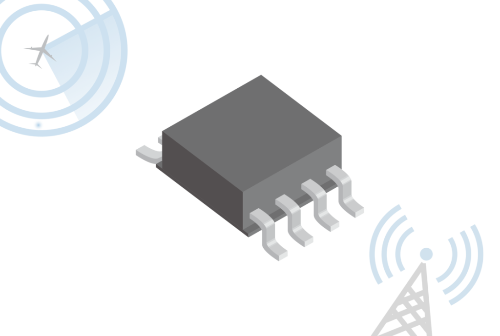
Samco offers process solutions of wide bandgap semiconductors including GaAs, GaN and InP for RF device production in the field of telecommunication and defense applications.
- Epi Growth
- SiO₂ Mask Fabrication for Ion Implantation
- Recess Etching for HEMT fabrication
- Contact Hole Formation by SiO₂ Etching
- Backside Via Hole Etching
- Plasma Dicing for Higher Yields