Samco's Process Expertise
At Samco, we take pride in our extensive process know-how and advanced capabilities in semiconductor and electronic component manufacturing. Our longstanding commitment to innovation and excellence has positioned us as a trusted partner for clients worldwide.
Since our establishment in 1979, Samco has built a reputation for excellence in deposition, etching, and surface treatment processes. Our decades of experience and dedication to research and development have enabled us to provide cutting-edge solutions for a wide array of applications. Our team of experts continuously develops new techniques to ensure we stay at the forefront of technology.
Choosing Samco means choosing expertise and innovation. From deposition and etching to surface treatment, we offer a full spectrum of processes to meet diverse manufacturing requirements. We provide tailored systems for both R&D and production, ensuring that our clients have the right tools for their specific needs. With business locations across the globe, we support clients worldwide with top-notch services and technical support. Our stringent quality control processes and dedication to excellence guarantee superior results for every project.
At Samco, we are passionate about pushing the boundaries of technology and delivering unparalleled process solutions. Explore our expertise and discover how we can help you achieve your manufacturing goals.
Featured Solutions
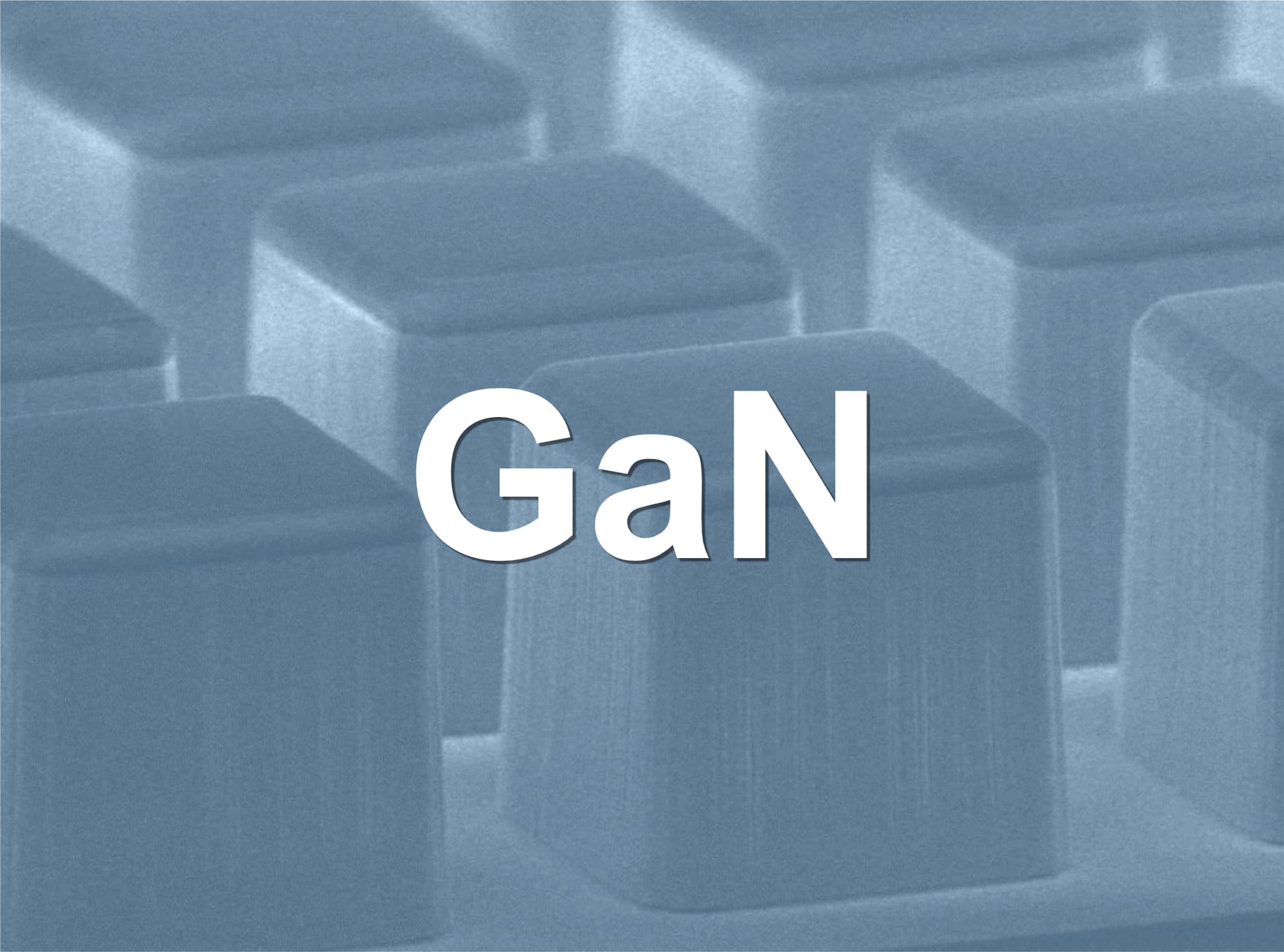
Gallium Nitride (GaN) Etching
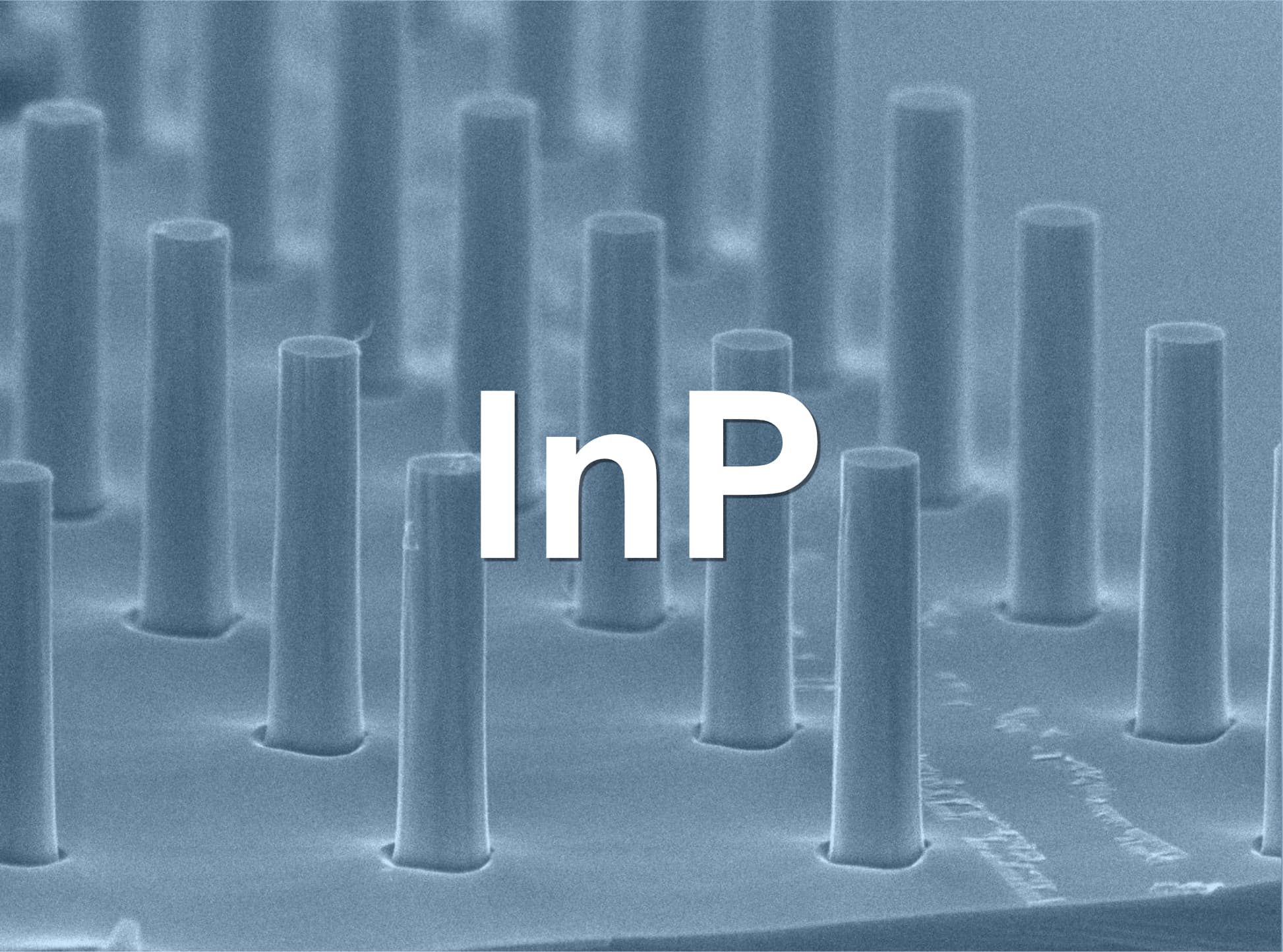
Indium Phosphide (InP) Etching
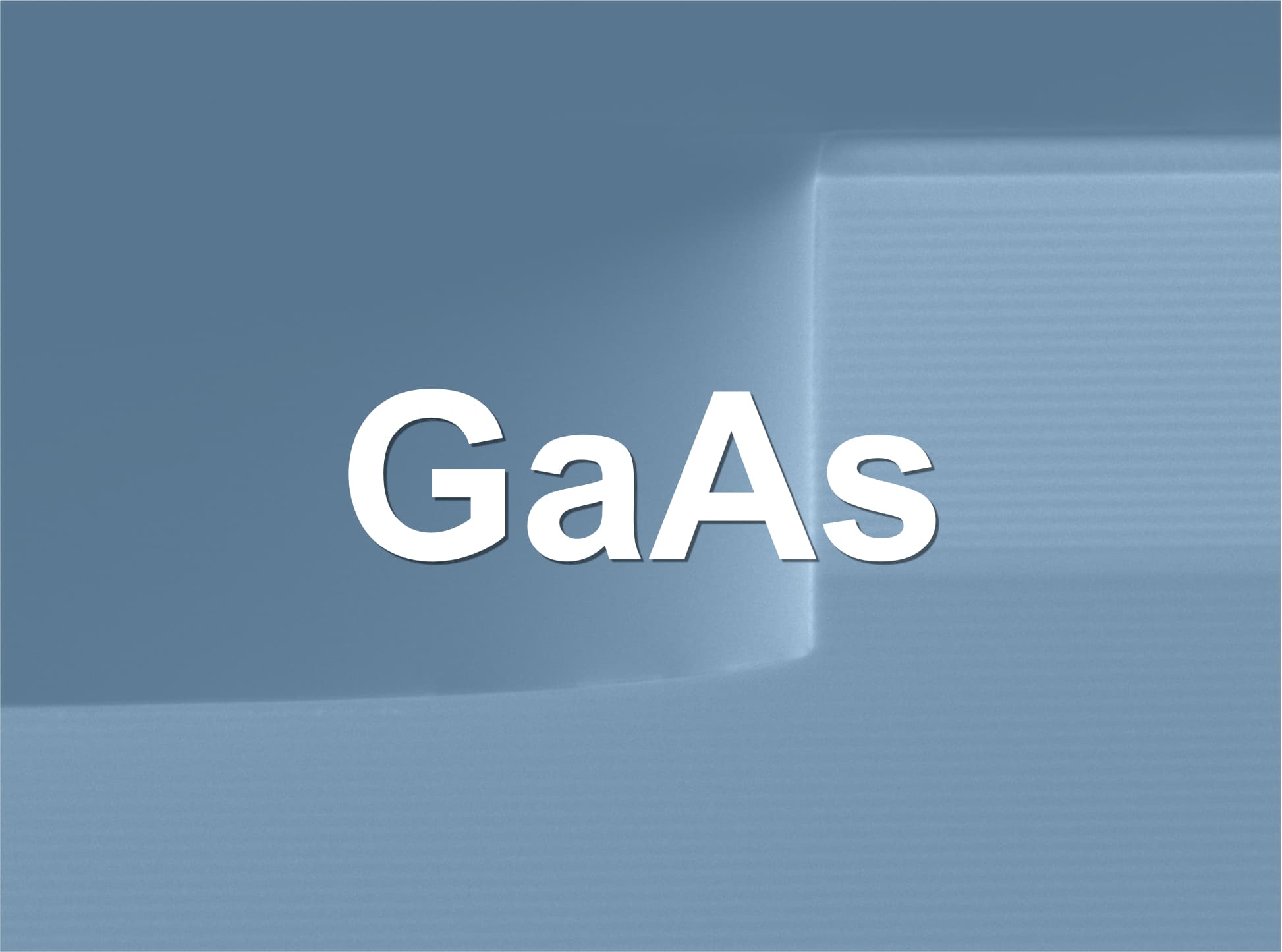
Gallium Arsenide (GaAs) Etching
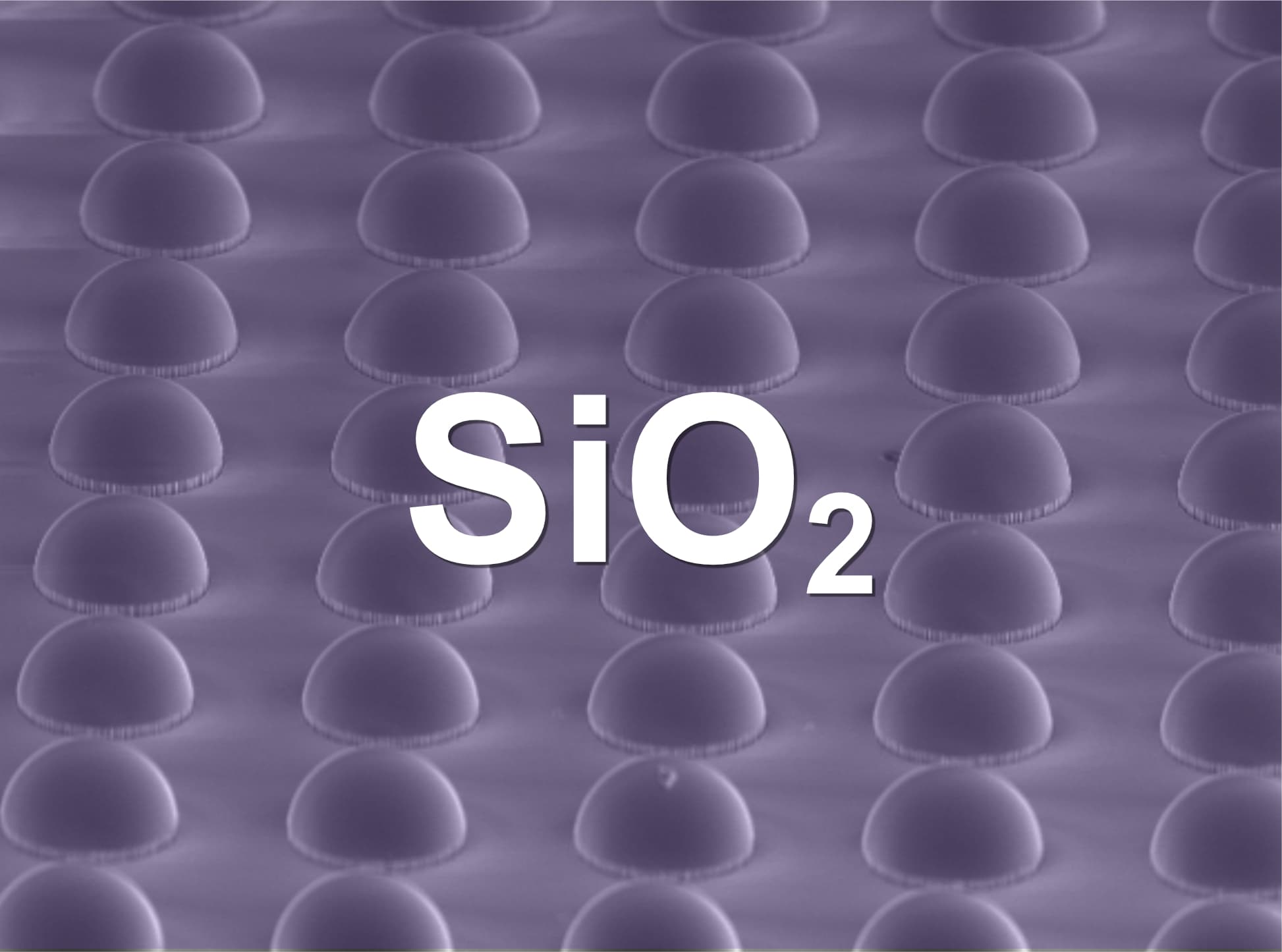
SiO2 deposition
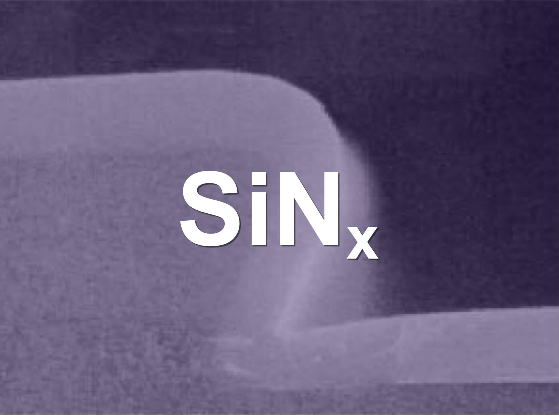
SiNx deposition
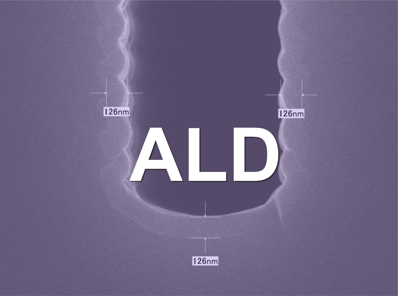
Atomic Layer Deposition (ALD)
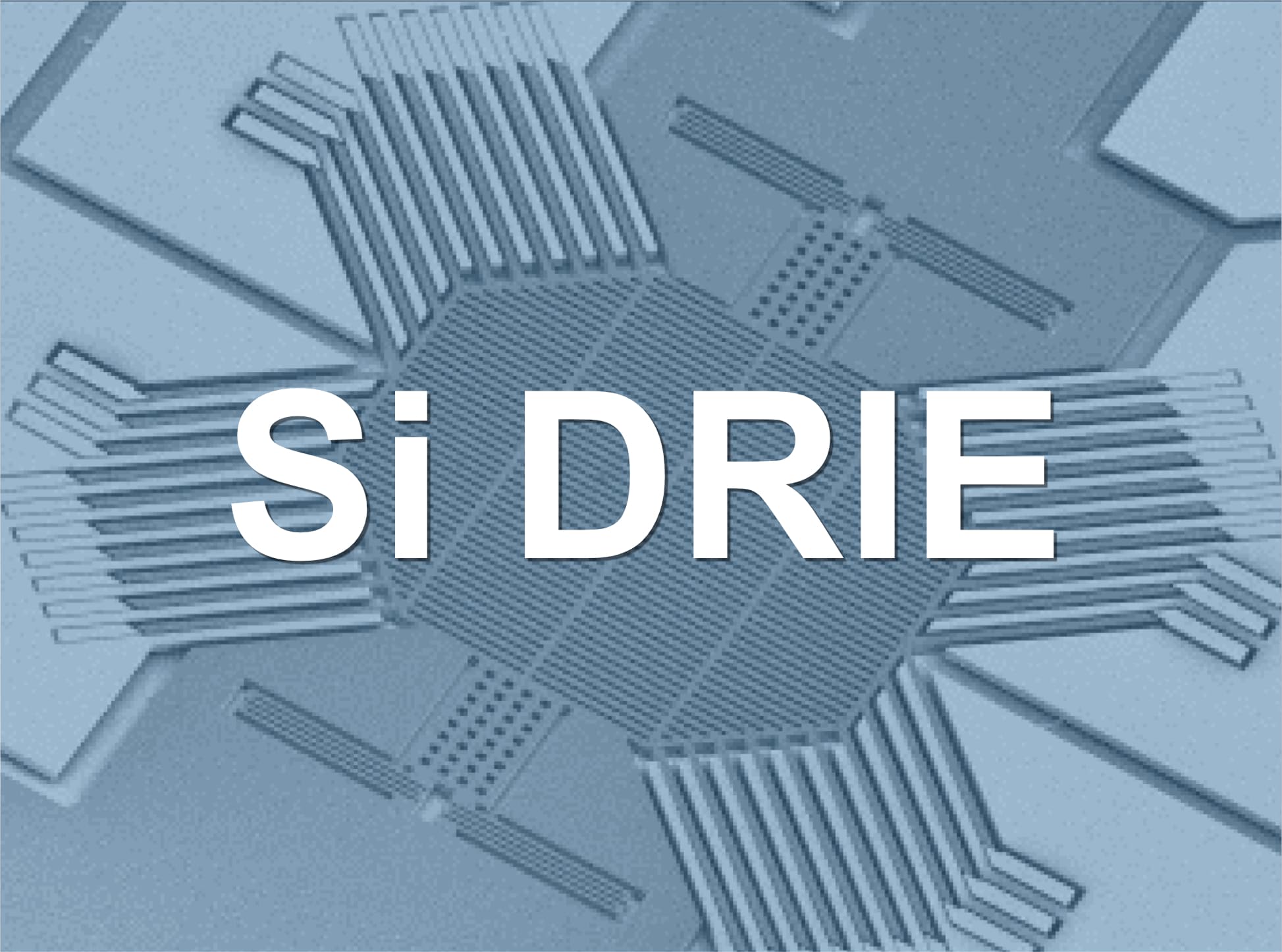
Silicon Deep Reactive Ion Etching (DRIE)
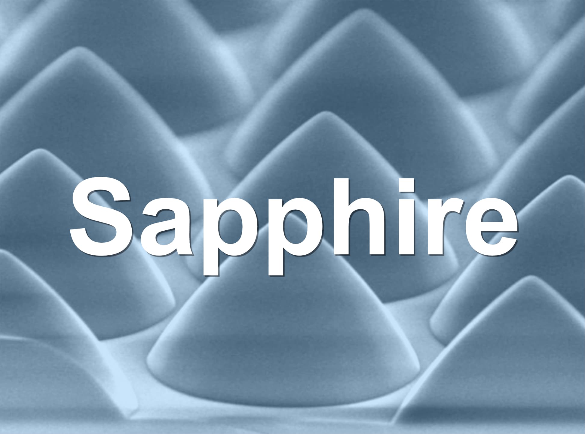
Sapphire Etching
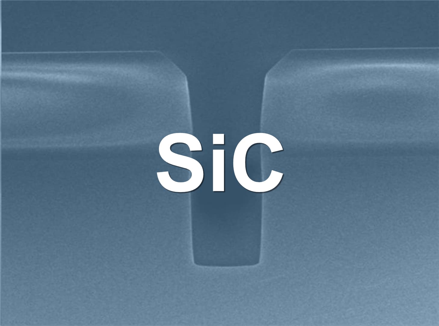
SiC Etching
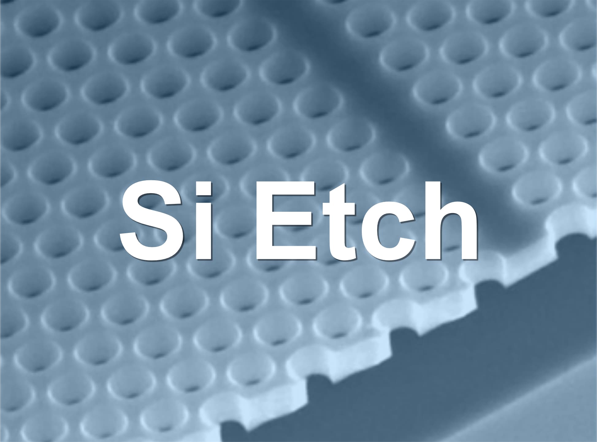
Si Etching
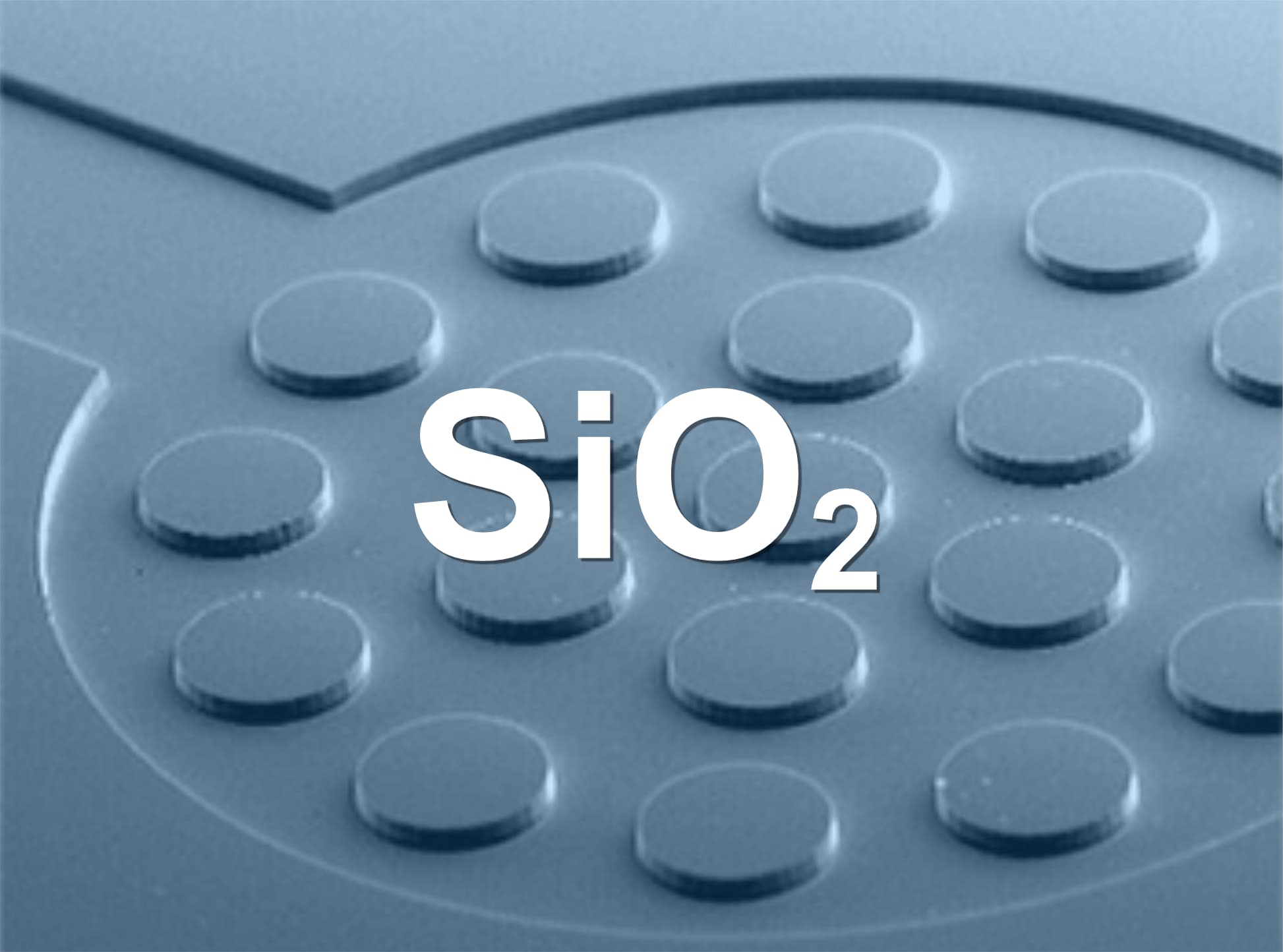
SiO2 Etching
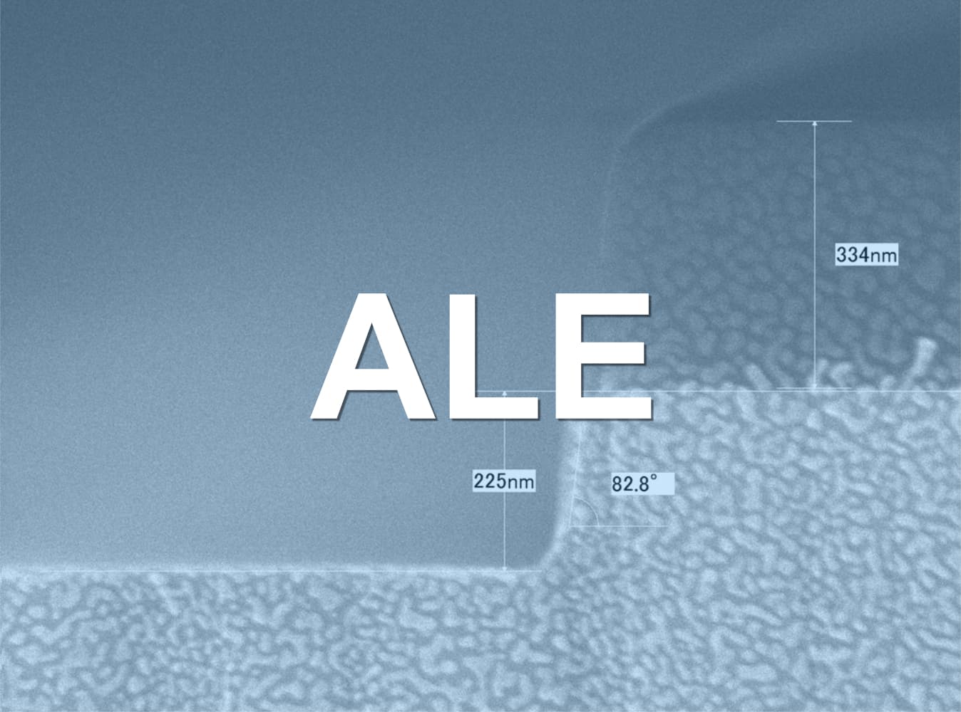
Atomic Layer Etching (ALE)
Deposition
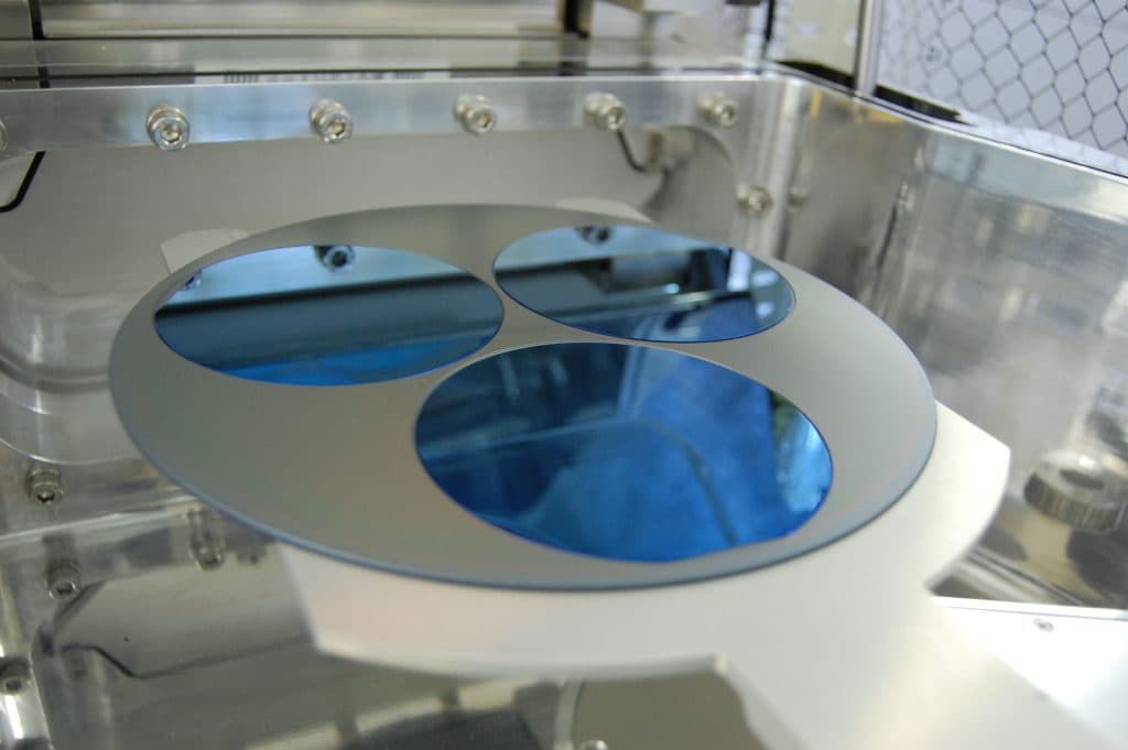
Our deposition processes include Atomic Layer Deposition (ALD), Plasma Enhanced Chemical Vapor Deposition (CVD) including Anode PECVD and Cathode PECVD, and Diamond-Like Carbon (DLC) Coating. These methods allow us to achieve precise film growth with exceptional uniformity and thickness control. Whether it’s depositing thin films or creating extremely thick films, our deposition systems are designed to meet the stringent requirements of modern semiconductor manufacturing.
Etching
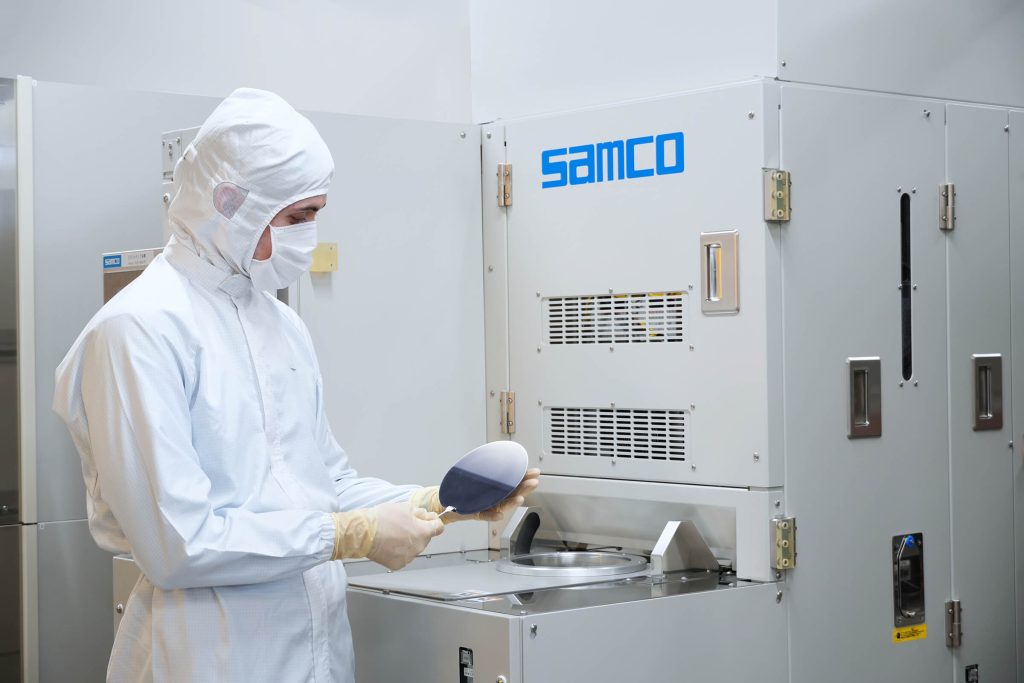
Samco’s etching processes are renowned for their precision and versatility. We offer Atomic Layer Etching (ALE), Inductively Coupled Plasma (ICP) Etching, Deep Reactive Ion Etching (DRIE), Reactive Ion Etching (RIE), and Xenon Difluoride Etching. Our expertise spans a variety of materials, including GaN, GaAs, InP, Si, SiO₂, and SiC, making us a trusted partner for compound semiconductor applications, MEMS, RF filters, and more.
Surface Treatment
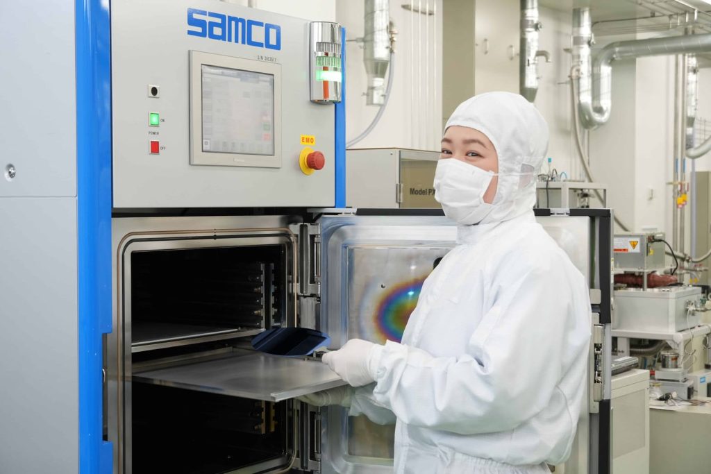
We provide advanced surface treatment processes, including Aqua Plasma® Cleaning, Plasma Cleaning, and UV Ozone Cleaning. These methods effectively remove organic contaminants and prepare surfaces for subsequent manufacturing steps. Our proprietary Aqua Plasma® technology and UV Ozone Cleaners ensure thorough and environmentally friendly cleaning solutions, catering to both R&D and high-volume production needs.
