Plasma Dicing/Scribing of Silicon & III-V (GaAs/InP/GaN)
SAMCO Inc. > Featured Solutions > Plasma Dicing/Scribing
In the back-end process community, the damage on dies during blade dicing is a serious issue. As a pioneer of etching process solutions of various materials, Samco has developed plasma dicing solutions for some of our customers looking to improve yields. This technology can be applied to a wide variety of applications including RF devices and HB LEDs production.

Challenges using Blade Dicing Techniques
Blade dicing has been used for the die preparation process, the technology is facing some tough challenges to meet demands for next-generation device manufacturing process.
1. Chipping and cracking of dies
When a wafer is thinned, the chance of defects due to chipping and cracking increases.
2. More streets, lower process throughput
In the case of smaller die separation, the blade needs to go through all the streets of wafers.
3. Limitation in street width
Kerf width of the blade determines the street width (generally over 70 μm).
4. Limitation in die shape
Square shape is typical due to grid-style streets.
5. Mechanical stress of dies
The Grid-style streets by blade dicing cannot mitigate the stress of the dies.
6. Limitation in processed materials
Dicing blades cannot handle with brittle materials such as Indium Phosphide (InP) and Gallium Arsenide (GaAs).
Samco’s Plasma Dicing Capabilities
Customized Plasma Dicing Solutions
Samco offers process solutions of “Dicing Before Grinding” (DBG) or “Scribe and Break”. These processes are specially developed and customized to meet our customers’ requests.


Dicing Before Grinding (DBG) Process
Dies are processed half-cut by plasma etching before grinding.
Damage Free Process
Narrow Street Width
Samco’s plasma dicing process shows advantages on street width over conventional blade dicing process.
The plasma-based process allows the street design which cannot be produced using conventional blade dicing processes.

Simultaneous Die Separation on a Wafer
The simultaneous processing of all streets by dry etching gives higher throughput compared with blade dicing, especially for large-wafer dicing with long street lines.

Stress Mitigation of Dies
Die stress can be mitigated by using a special dicing process in combination with the etch mask design.

Dicing of Various Materials
Samco can process wafers with various materials such as Silicon (Si), Gallium Arsenide (GaAs), Indium Phosphide (InP), Gallium Nitride on Silicon (GaN-on-Si), wafers with metal or resin layers.
For our process capabilities of GaAs wafer processing, please check the technical notes below,
• GaAs Wafer Plasma Scribing with ICP Etching

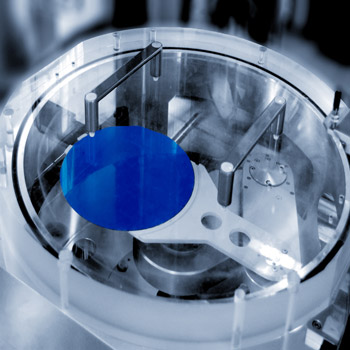
Applicable to Small-size Wafers
Samco plasma etchers can be configured for single-wafer or batch processing using a wafer carrier. Brittle substrates such as Indium Phosphide (InP) and Gallium Arsenide (GaAs) can be handled without the risk of breaking.

The Value of Samco’s Processes
 Die yield improvement
Damage-free die processing enhances productivity.
Creation of any die shape
Circular, hexagonal shape or multiple-size dies on a wafer can be processed simultaneously.
Process support from R&D to production
Multiple system line-up enables easy switching from R&D to production.
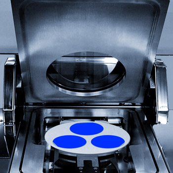
System Lineup
ICP Etch Systems for Batch Processing
– Capable of batch processing of small wafers
– Suitable for dicing of compound semiconductor materials