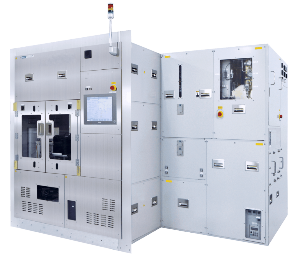
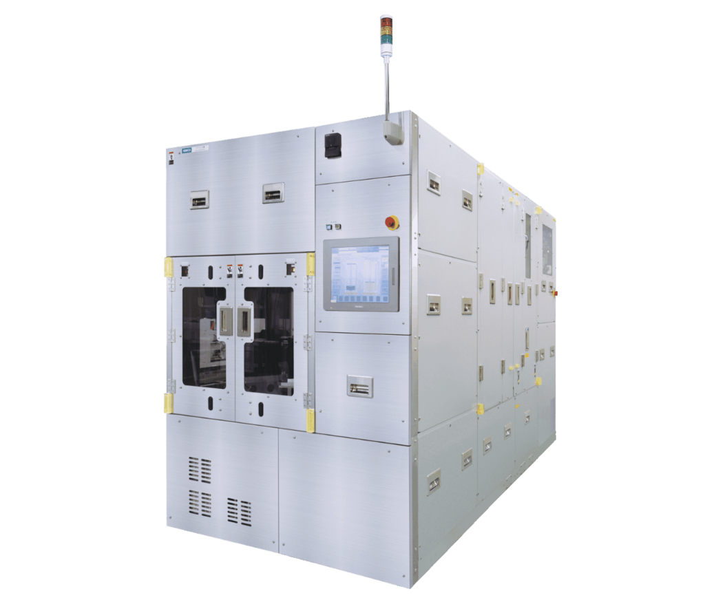
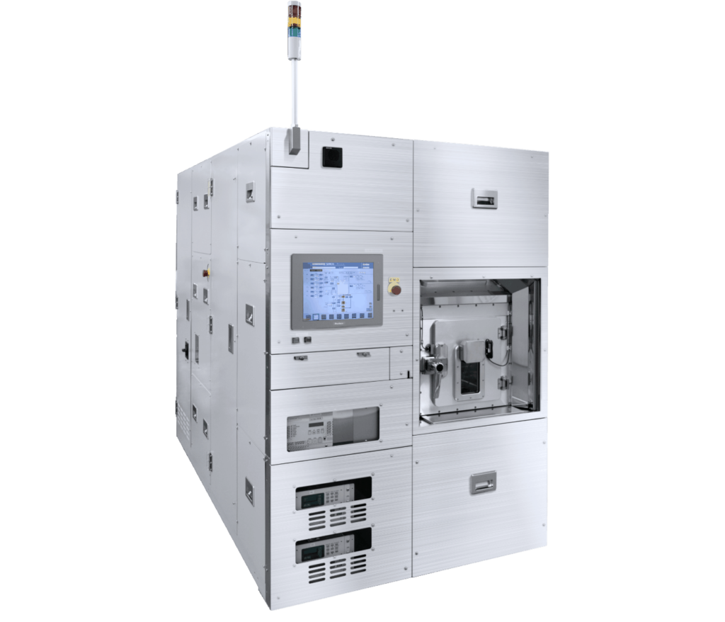
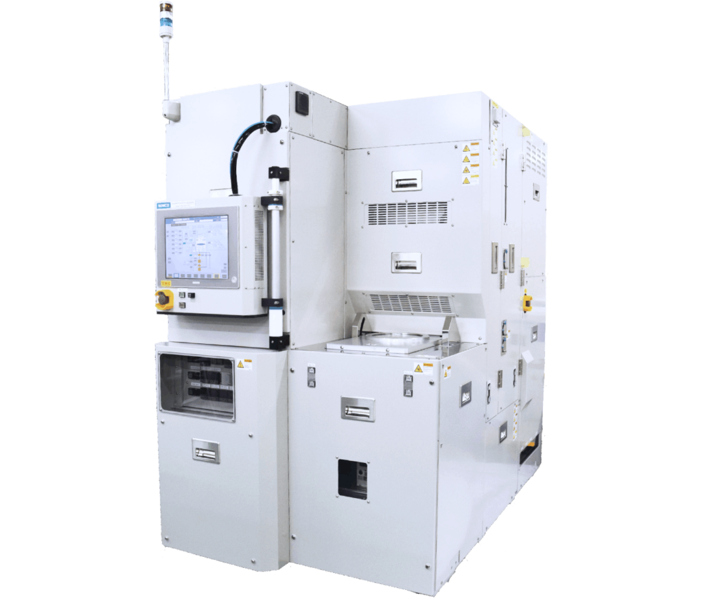
Category: Si DRIE
Scientific paper on PZT ultrasonic microsensors by Kyoto Institute of Technology
Sensitivity of Piezoelectric Ultrasonic Microsensors with Sol-Gel Derived PZT Films Prepared through Various Pyrolysis Temperatures
Kaoru Yamashita, Shota Nakajima, Jo Shiomi and Minoru Noda
Graduate School of Science and Technology, Kyoto Institute of Technology, Kyoto 606-8585, Japan
2017 IEEE International Meeting for Future of Electron Devices, Kansai (IMFEDK), Kyoto, Japan, 2017, pp. 108-109.
In this paper, MEMS ultrasonic microsensors with sol-gel derived PZT piezoelectric diaphragm was fabricated. In device fabrication, Samco silicon Deep RIE etcher RIE-400iPB was used to form the thin diaphragm structure by silicon plasma etching from the wafer backside.
Stress control of PZT thin film was carried out to investigate high ultrasonic sensitivity of the devices.
Samco provides silicon deep RIE etching technologies utilizing the Bosch Process to R&D labs for MEMS device and TSV processing applications. For more information on our process technologies of deep silicon etching, please visit the process data page below.
Silicon Deep RIE Process Data
Scientific paper on micro-scale corral fabrication by Princeton University
Bacterial population solitary waves can defeat rings of funnels
Ryan J Morris1, Trung V Phan2, Matthew Black3, Ke-Chih Lin4, Ioannis G Kevrekidis5, Julia A Bos3 and Robert H Austin2
1 School of Physics & Astronomy, University of Edinburgh, Edinburgh EH9 3FD, United Kingdom
2 Department of Physics, Princeton University, Jadwin Hall, Princeton, NJ 08544, United States of America
3 Lewis-Sigler Institute for Integrative Genomics, Princeton, NJ 08544 United States of America
4 Department of Electrical Engineering, Princeton University, Princeton, NJ 08544, United States of America
5 Department of Chemical and Biological Engineering and PACM, Princeton University, Princeton, NJ 08544, United States of America
New Journal of Physics (2017) Volume 19 035002
Circular corral for bacteria made of rings of concentric funnels was fabricated. Nanoslits were etched on a silicon wafer using Samco Deep RIE Tool RIE-800iPB at Princeton University.
Samco offers a couple of silicon Deep RIE systems for R&D and production. Please see the product page below.
Silicon Deep RIE Systems
Also, for more details of Samco silicon deep RIE process capabilities, please visit the process solution page below.
Slicon Deep RIE Technology for MEMS and TSV Processing
Scientific Paper on Microfluidic Chip Fabrication Using Silicon Deep RIE from Vietnam National University
Fabrication of 25 μm-filter microfluidic chip on silicon substrate
Nguyen Ngan Le1,2, Kim Khanh Huynh1, Thi Cam Hue Phan1, Thi My Dung Dang1 and Mau Chien Dang1
1 Laboratory for Nanotechnology, Vietnam National University in Ho Chi Minh City, Community 6, Linh
Trung Ward, Thu Duc District, Ho Chi Minh, Vietnam
2 University of Science, Vietnam National University in Ho Chi Minh City, 227 Nguyen Van Cu Street,
District 5, Ho Chi Minh City, Vietnam
Adv. Nat. Sci.: Nanosci. Nanotechnol. 8 (2017) 015003
A microfluidic chip device was fabricated using deep silicon etching technology of the Bosch Process. Samco Deep RIE Tool RIE-200iPB was used for silicon etching over silver hard mask. With optimization of process recipe in the silicon etching, vertical silicon channel profile was fabricated.
For more details of our deep RIE process capabilities, please visit the pages below.
Silicon DRIE (Deep Reactive Ion Etching) for MEMS and TSV
Deep Silicon Trench/Via Hole/Pillar Etching using the Bosch Process
Scientific Paper on MEMS Diaphragm Sensor from Kyoto Institute of Technology
Influence of top electrodes to vibration modes in impulse responses of MEMS piezoelectric diaphragms for ultrasonic microsensors
T. Nishioka, T. Nishiumi, K. Yamashita and M. Noda
Graduate School of Science and Technology, Kyoto Institute of Technology, Matsugasaki, 606-8585, Japan
2016 IEEE International Meeting for Future of Electron Devices, Kansai (IMFEDK), Kyoto, 2016, pp. 1-2.
doi: 10.1109/IMFEDK.2016.7521705
Ultrasonic micro sensors with piezoelectric diaphragms were fabricated to investigate the relationship between vibration mode and device structure of electrode and the diaphragms. Samco Deep Reactive Ion Etching system was used for anisotropic silicon plasma etching in the Bosch Process over SiO2 mask.
For more details of our silicon plasma etching capabilities, please visit the process data pages below.
Silicon Plasma Etching Process Data (RIE and ICP-RIE)
Silicon Deep RIE Process Data Using the Bosch Process
Scientific Paper on Silicon Nanowire Fabrication Using the Bosch Process by Kyoto University
Tensile fracture of integrated single-crystal silicon nanowire using MEMS electrostatic testing device
Toshiyuki Tsuchiya , Tetsuya Hemmi, Jun-ya Suzuki, Yoshikazu Hirai, Osamu Tabata
Department of Micro Engineerng, Kyoto University, Kyotodaigaku-Katsura C3, Nishikyo-ku, Kyoto 615-8540, Japan
Procedia Structural Integrity (2016) 2 Pages 1405–1412
Samco silicon Deep RIE system at Kyoto University was used for silicon nanowire fabrication by combination of two types of silicon etch processes (the Bosch Process) with coarse and fine scallops. Using the unique silicon plasma etching processes, silicon nanowire structures were successfully fabricated on a SOI wafer.
Kyoto University is one of Samco Deep RIE system customers for MEMS device research.
For more details of our silicon Deep RIE process technologies, please visit the process data pages below.
Silicon Deep RIE for MEMS & TSV Applications
Deep Silicon Etching Using the Bosch Process – Trench, Via Hole & Pillar Etching
Also, For more information of our silicon Deep RIE systems, please visit the product page below.
Silicon Deep RIE Systems
Scientific Paper on Plasmonic Array with Mesoporous Silica Layer Fabrication by Kyoto University
Mesoporous silica layer on plasmonic array: light trapping in a layer with a variable index of refraction
Shunsuke Murai1, 2, Hiroyuki Sakamoto1, Koji Fujita1, and Katsuhisa Tanaka1
1 Department of Material Chemistry, Graduate School of Engineering, Kyoto University, Katsura, Nishikyo-ku, Kyoto, 615-8510, Japan
2 PRESTO, Japan Science and Technology Agency (JST), Kawaguchi, Saitama 332-0012, Japan
Optical Materials Express Vol. 6, Issue 9, pp. 2736-2744 (2016) doi: 10.1364/OME.6.002736
Plasmonic array was fabricated using nanoimprint technology. First, silicon mold consisting of a periodic square array was fabricated using silicon deep etching. Samco silicon DRIE system at Kyoto University was used for the mold fabrication. Then, Samco ICP etch system was used for pattern transfer by aluminum dry etching over photoresist pattern fabricated by the nanoimprint process.
Scientific Paper on Atomically Ordered Silicon Side-surface Structures From Osaka University Team
Methods of creating and observing atomically reconstructed vertical Si{100}, {110}, and {111} side-surfaces
Azusa N. Hattori1,2, Shohei Takemoto3, Ken Hattori3, Hiroshi Daimon1 and Hidekazu Tanaka1
1 Nanoscience and Nanotechnology Center, The Institute of Scientific and Industrial Research, Osaka University, Ibaraki, Osaka 567-0047, Japan
2 JST-PRESTO, Kawaguchi, Saitama 332-0012, Japan
3 Graduate School of Materials Science, Nara Institute of Science and Technology, Ikoma, Nara 630-0101, Japan
Appl. Phys. Express (2016) 9 085501
Samco silicon Deep Reactive Ion Etch (DRIE) system at Osaka University was used for silicon nano-scale structure fabrication.
For our process examples and capabilities of deep silicon etching using Bosch Process, please visit the pages below.
Deep Silicon Trench/Via Hole Etching using Bosch Process
Si DRIE (Deep Reactive Ion Etching) for MEMS and TSV
Scientific Paper on Hybrid Silicon/Polymer Ring Resonator Fabrication from Kyushu University Team
Athermal Hybrid Silicon/Polymer Ring Resonator Electro-optic Modulator
Feng Qiu1, Andrew M. Spring1, Hiroki Miura2, Daisuke Maeda3, Masa-aki Ozawa3, Keisuke Odoi3, and Shiyoshi Yokoyama1, 2
1 Institute for Materials Chemistry and Engineering, Kyushu University, 6-1 Kasuga-koen Kasuga-city, Fukuoka 816-8580, Japan
2 Department of Molecular and Material Sciences, Kyushu University, 6-1 Kasuga-koen Kasuga-city, Fukuoka 816-8580, Japan
3 Nissan Chemical Industries, LTD, 2-10-1 Tuboi Nishi, Funabashi, Chiba 274-8507, Japan
ACS Photonics
DOI: 10.1021/acsphotonics.5b00695
Silicon plasma etching was performed using Samco silicon DRIE system to fabricate a hybrid silicon/polymer ring resonator electro-optic (EO) modulator.
For our process examples of silicon plasma etching, please visit process data page below.
Si Dry Etching Process (RIE, ICP-RIE or XeF2 Etch)
Deep Silicon Trench/Via Hole Etching using Bosch Process
Si DRIE (Deep Reactive Ion Etching) for MEMS and TSV
Scientific Paper on TiN Nanoparticle Array Fabrication Process by Kyoto University
Plasmonic arrays of titanium nitride nanoparticles fabricated from epitaxial thin films
Shunsuke Murai, Koji Fujita, Yohei Daido, Ryuichiro Yasuhara, Ryosuke Kamakura, and Katsuhisa Tanaka
Shunsuke Murai1,2 Koji Fujita1,3> Yohei Daido1 Ryuichiro Yasuhara1 Ryosuke Kamakura1 and Katsuhisa Tanaka1
1 Department of Material Chemistry, Graduate School of Engineering, Kyoto University, Katsura, Nishikyo-ku, Kyoto 615-8510, Japan.
Optics Express Vol. 24, Issue 2, pp. 1143-1153 (2016) •doi: 10.1364/OE.24.001143
Titanium Nitiride (TiN) nanoparticle arrays were fabricated using nanoimprint technologies.
For nanoimprint mold fabrication, Samco deep silicon etching system at Kyoto University was used for nanostructure fabrication on silicon molds. After transferring of the silicon mold pattern to photoresist on TiN substrate, Samco ICP etching system at Kyoto University was used for TiN dry etching over photoresist to fabricate TiN nanoparticle arrays.
Scientific Paper on Microfluidic Device Fabrication from National Taiwan University
Enhancement of microfluidic particle separation using cross-flow filters with hydrodynamic focusing
Yun-Yen Chiu, Chen-Kang Huang, and Yen-Wen Lu
Department of Bio-Industrial Mechatronics Engineering, National Taiwan University, Taipei 10617, Taiwan, Republic of China
Biomicrofluidics (2016) 10, 011906
Samco silicon DRIE system at National Taiwan University was used for microchannel fabrication with crossflow filtration mechanism.
For more details of our deep silicon etching capabilities, please visit the process data pages below.
Deep Silicon Trench/Via Hole Etching using Bosch Process
Si DRIE (Deep Reactive Ion Etching) for MEMS and TSV