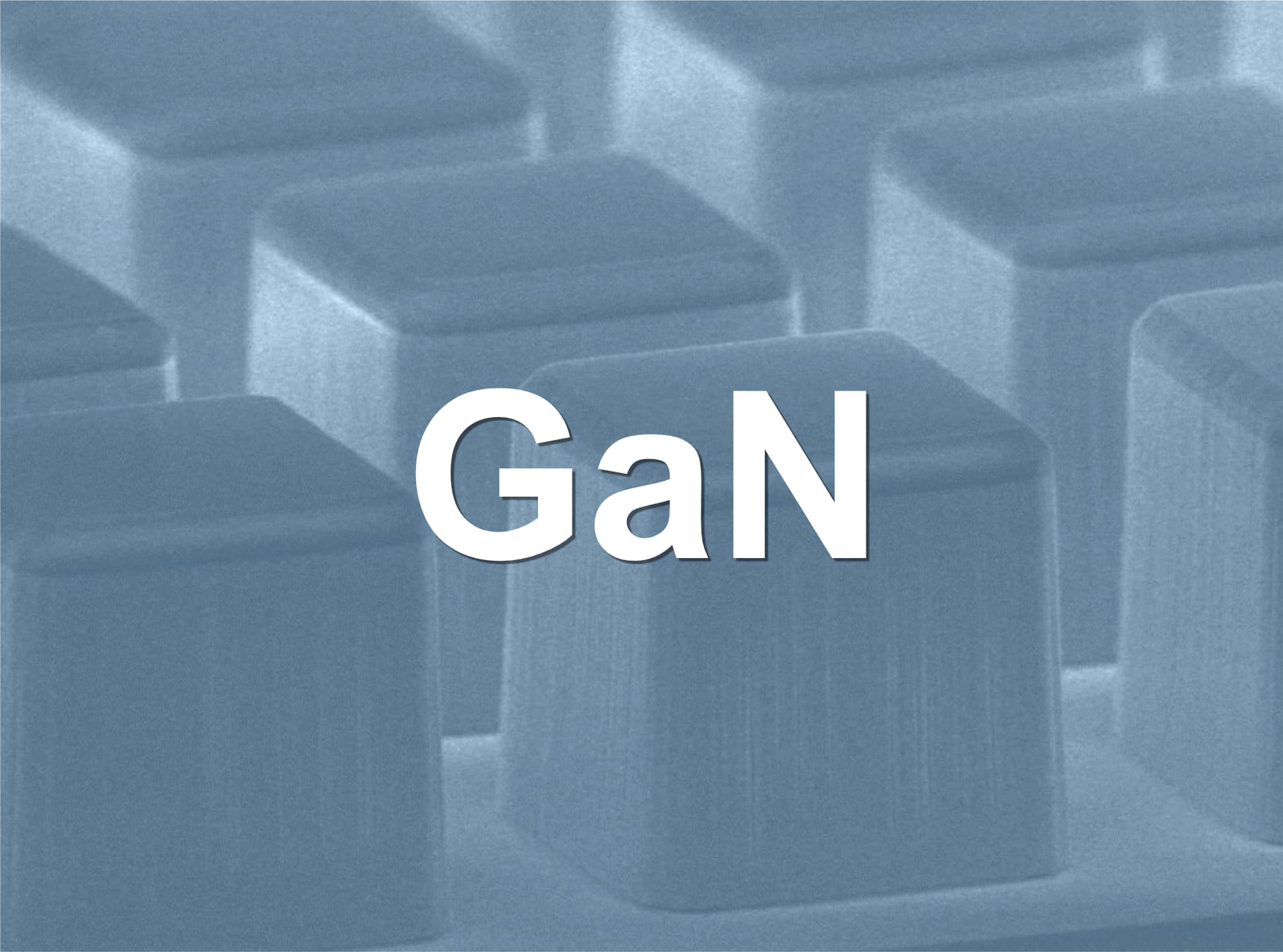
Gallium Nitride (GaN) Etching
GaN is a III-V compound semiconductor material which has wide band gap and high electron mobility. Applications include Vertical Power Devices, HB LEDs, and more.
Click Here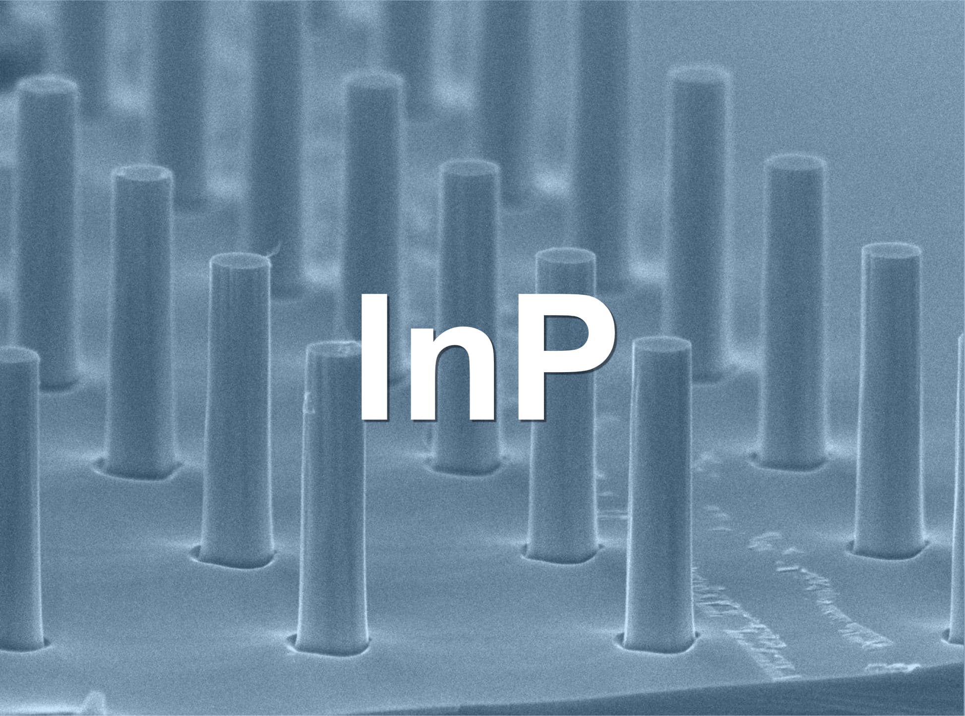
Indium Phosphide (InP) Etching
InP is a compound semiconductor material of III-V group. This material has a wide band gap and a high electron mobility.
Click Here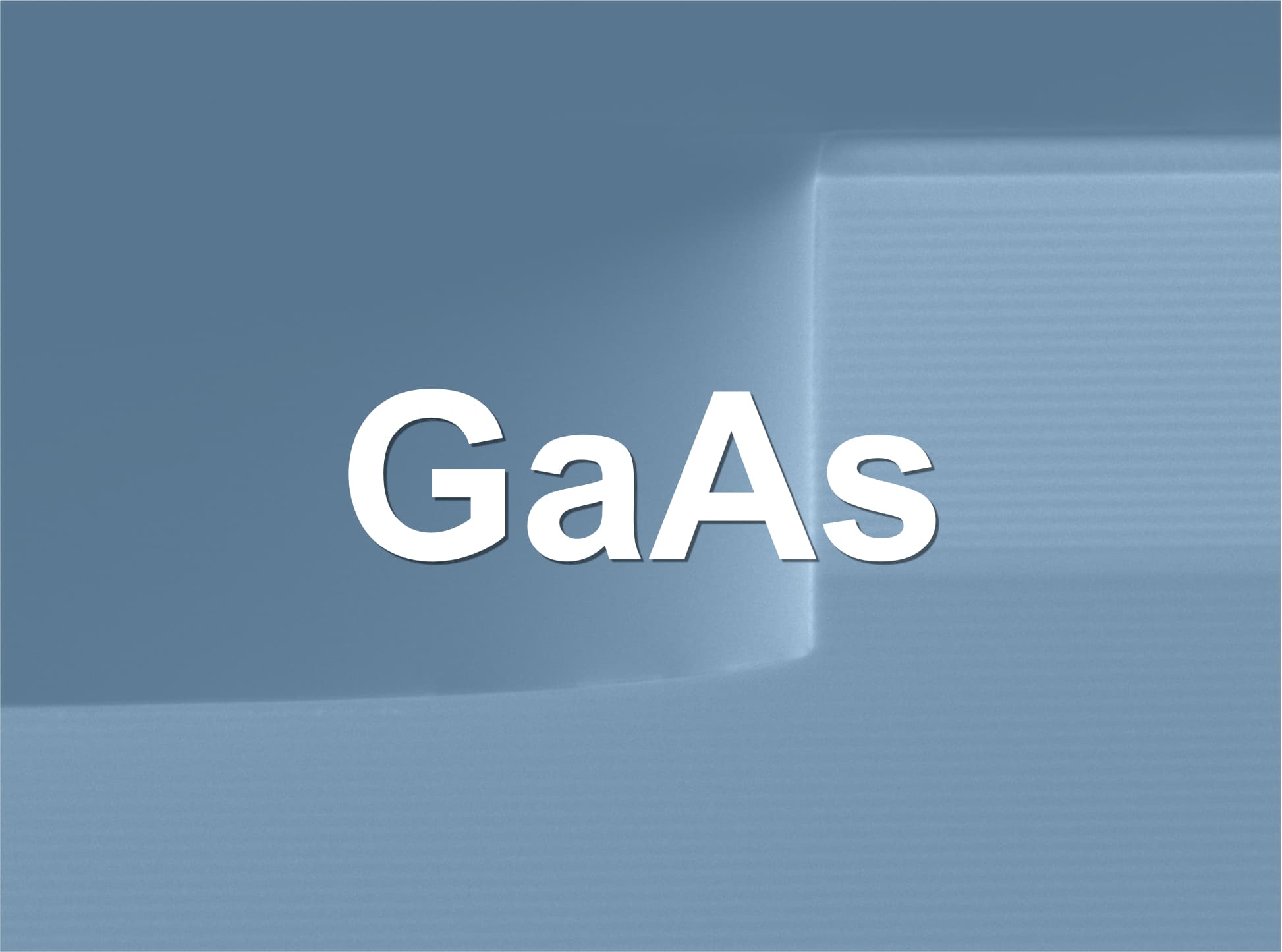
Gallium Arsenide (GaAs) Etching
GaAs is a III–V compound direct-gap semiconductor used for applications including optoelectronics and radio-frequency (RF) devices.
Button text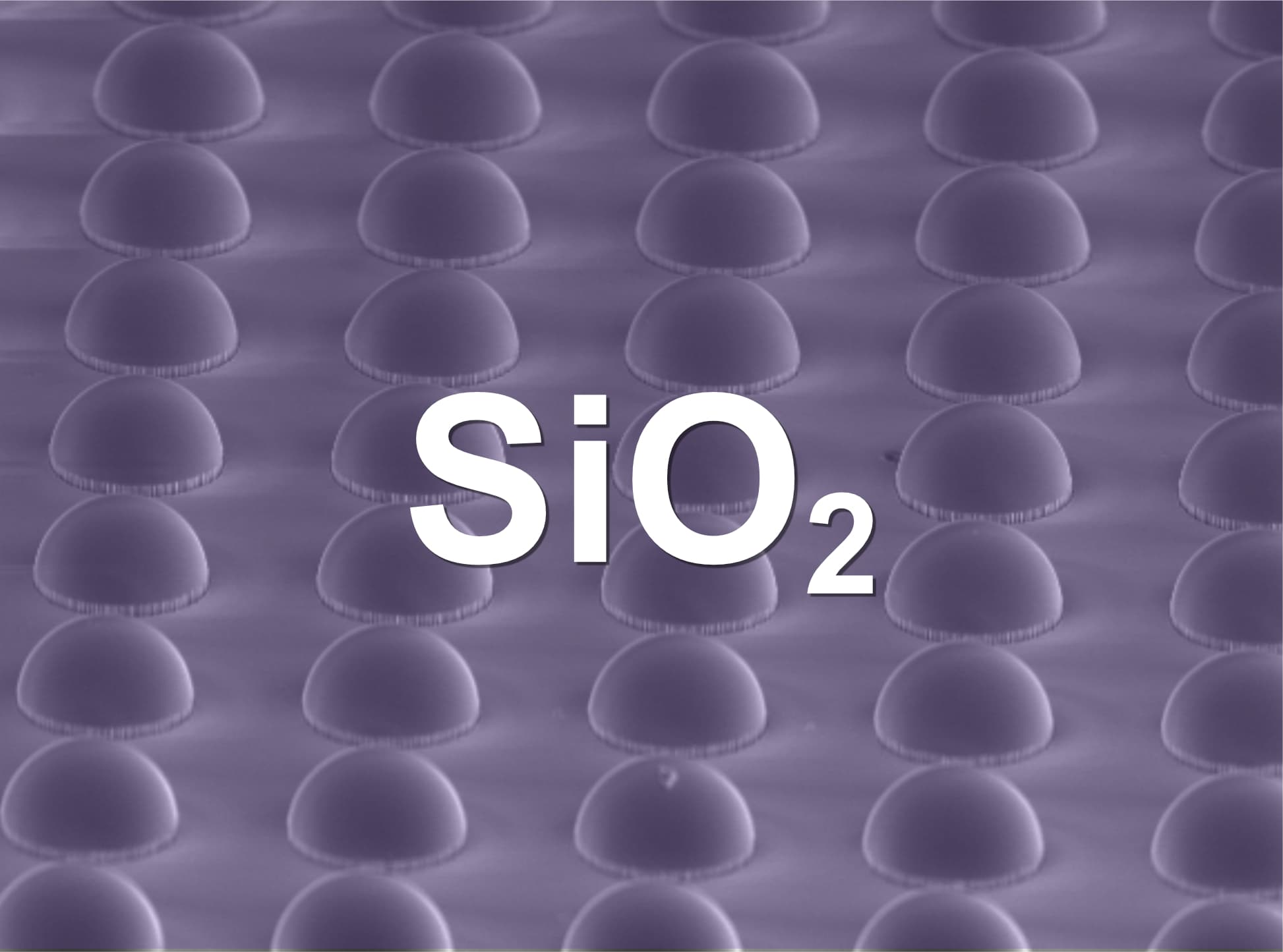
SiO2 deposition
SiO2 properties include excellent abrasion resistance, good electrical insulation, low thermal expansion and high thermal stability, making it ideal for a wide range of applications.
Button text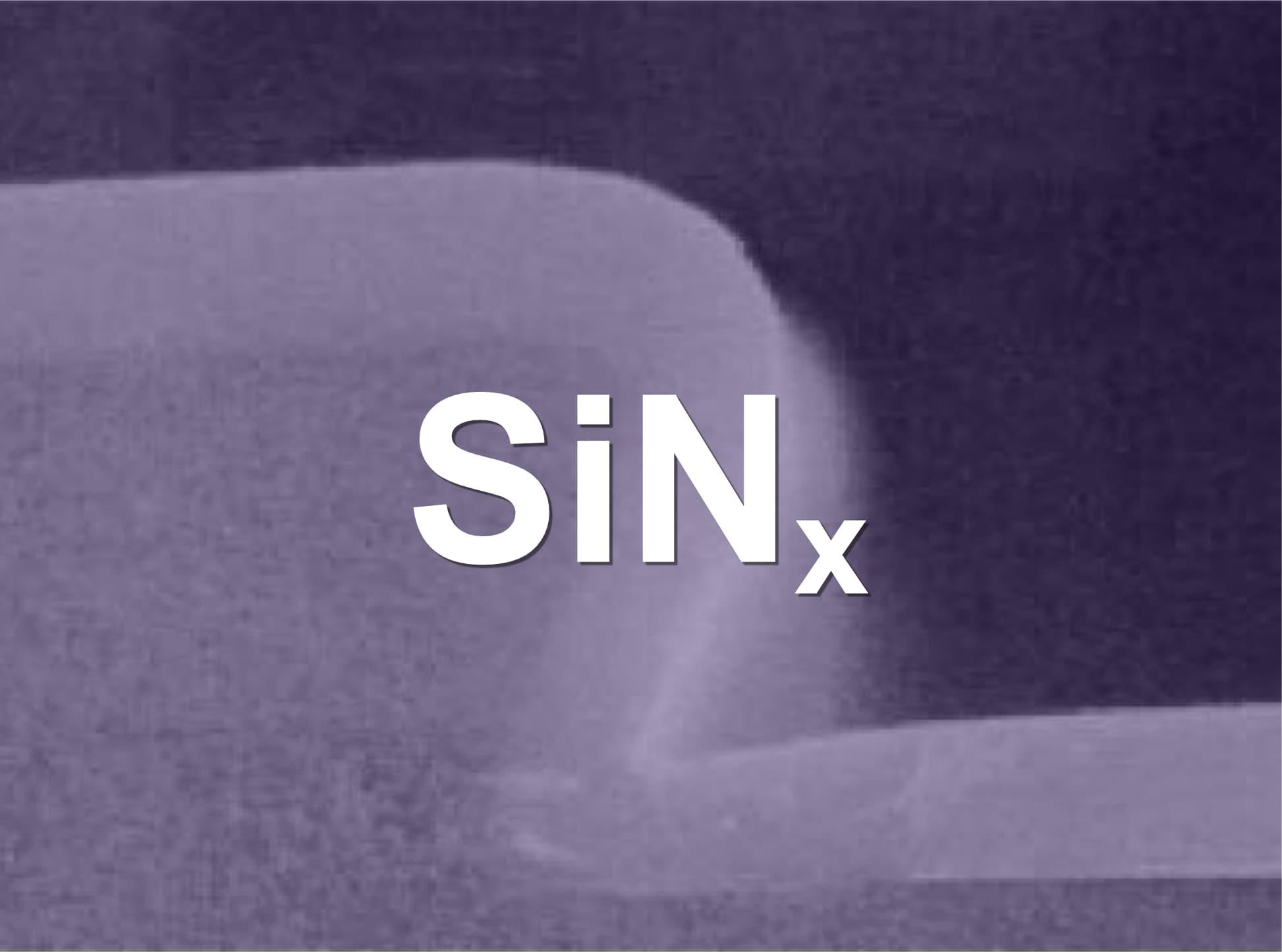
SiNx deposition
SiNx properties include low moisture and oxygen permeation, good electrical insulation and low thermal expansion. This material is used in a variety of applications in device fabrication.
Button text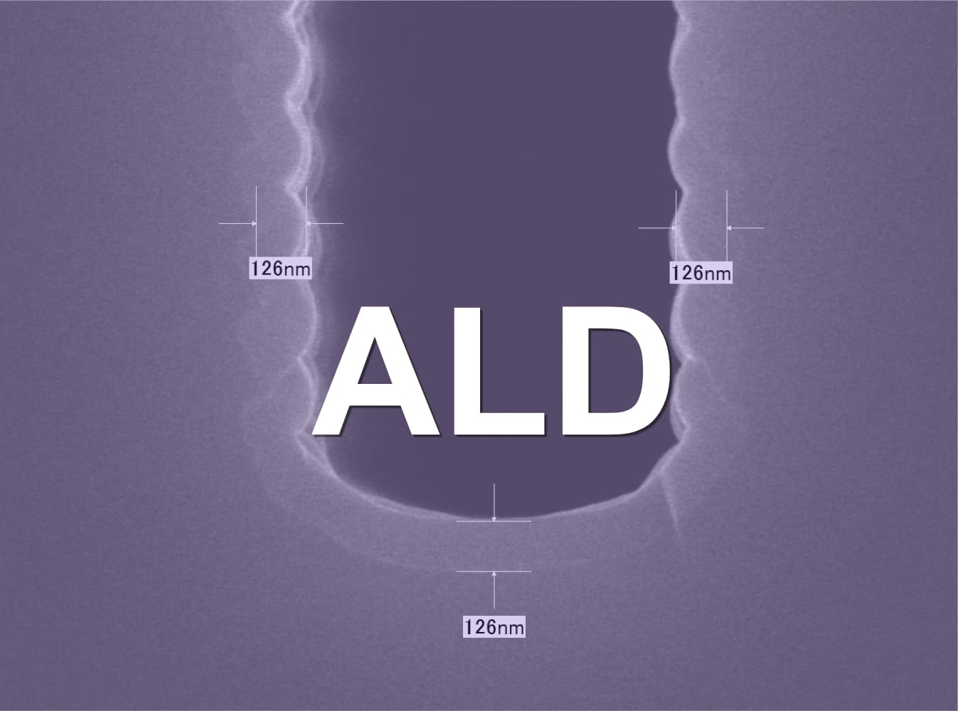
Atomic Layer Deposition (ALD)
ALD delivers uniform, pinhole-free films with precise thickness control, making it ideal for high-aspect-ratio and complex device structures.
Button text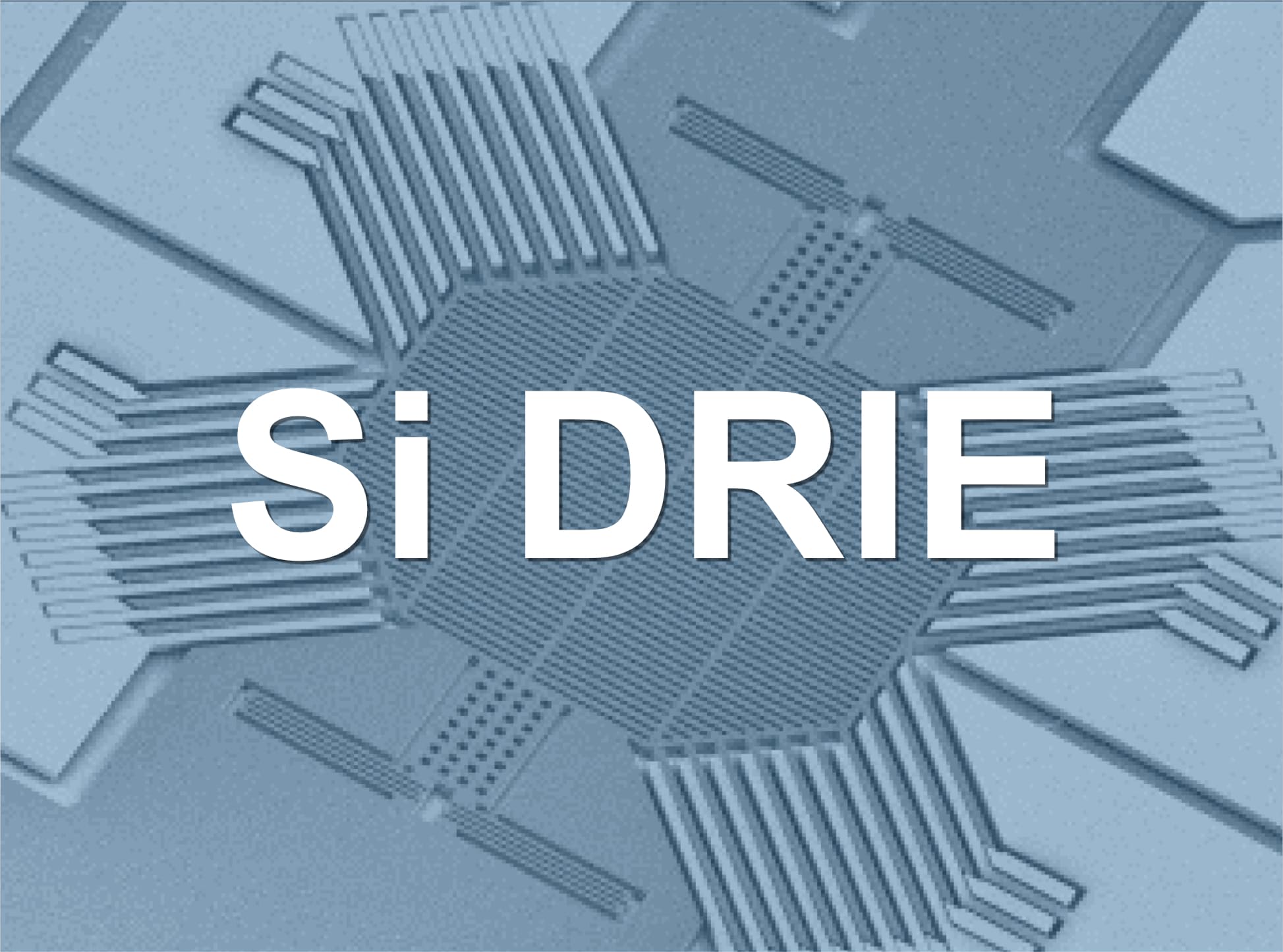
Silicon Deep Reactive Ion Etching (DRIE)
The Bosch Process enables deep silicon etching process solutions with high aspect ratio etching and excellent selectivity, ideal for MEMS and packaging applications.
Button text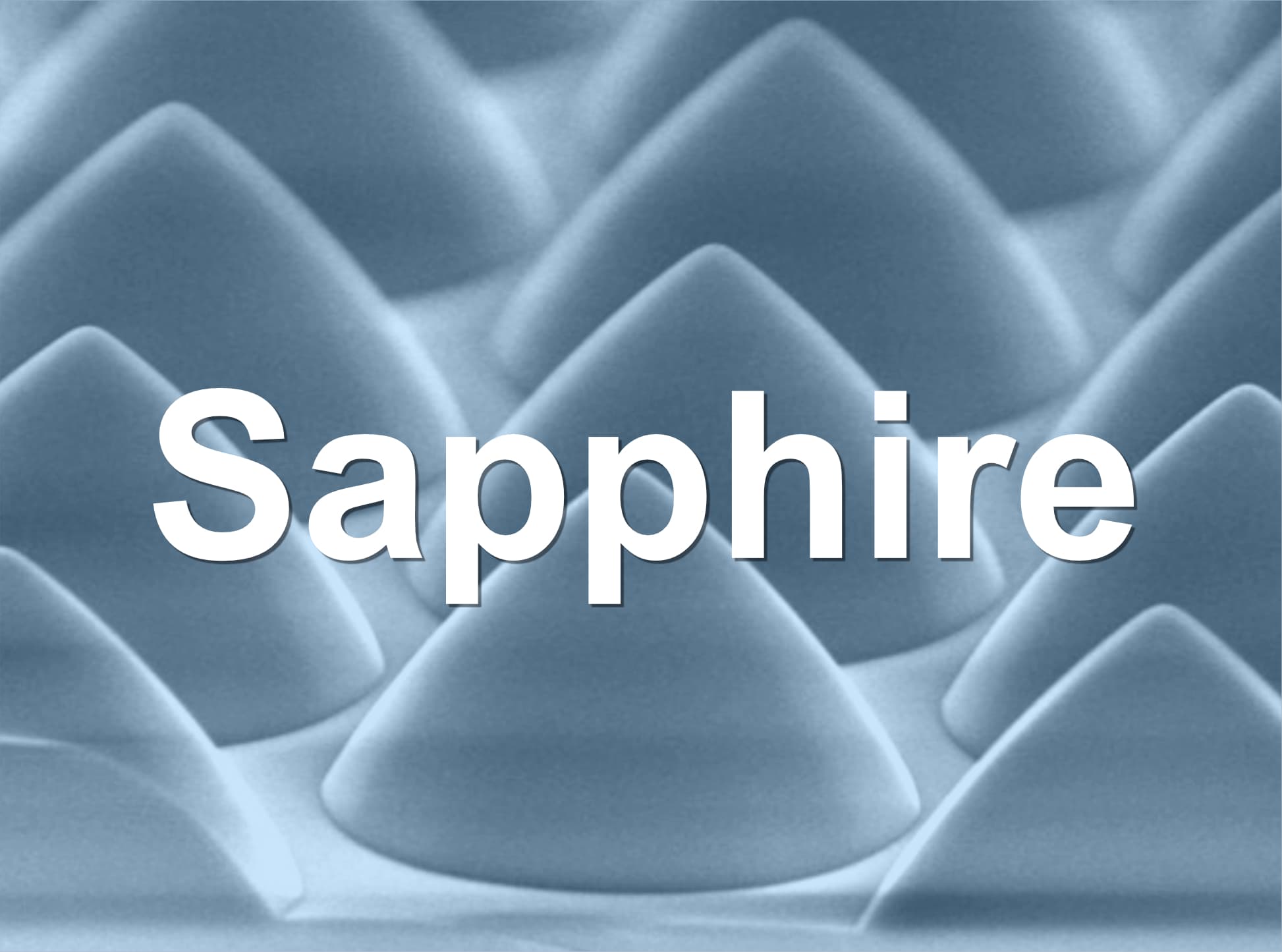
Sapphire Etching
Sapphire is a single crystal form of corundum, Al2O3. This material has unique material properties, especially for thermal stability, chemical stability, mechanical strength and optical properties.
Button text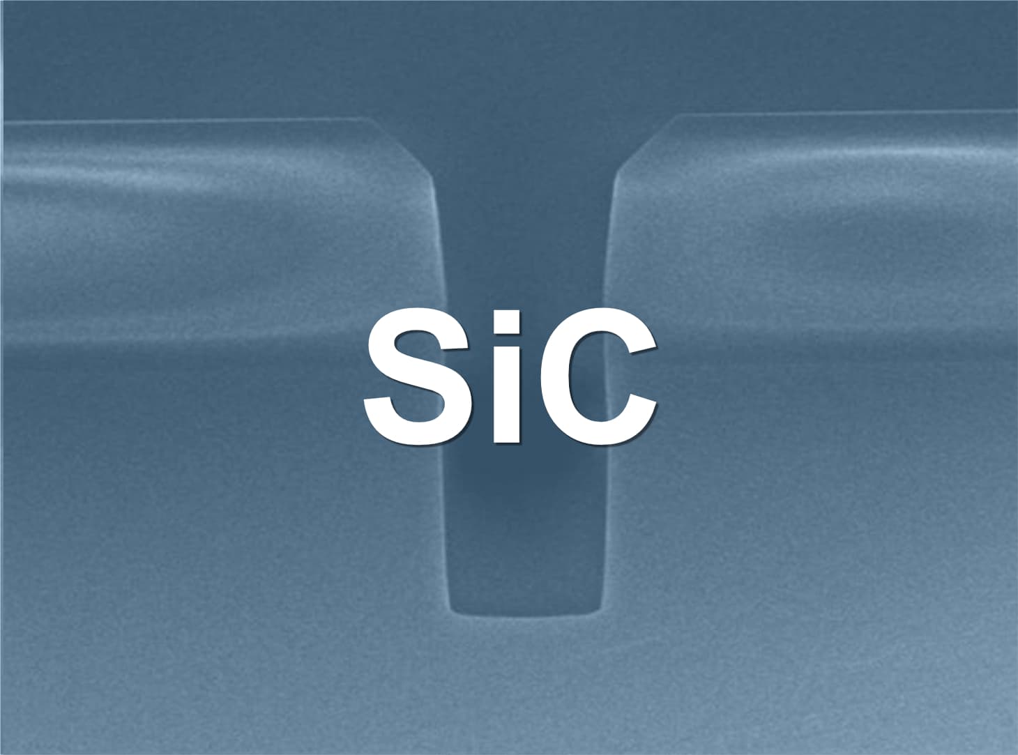
SiC Etching
Silicon Carbide (SiC) is a compound semiconductor material. The crystalline structure 4H-SiC is the most promising material as a substrate of power devices.
Button text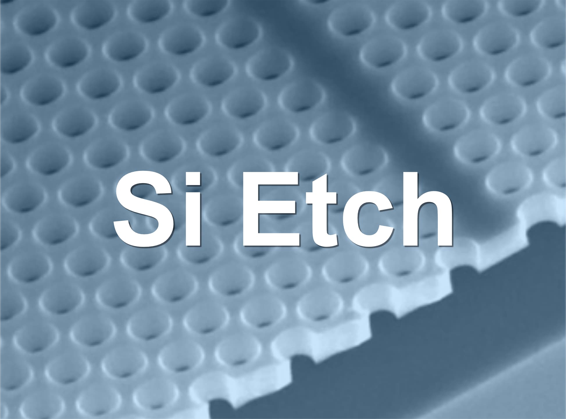
Si Etching
Crystalline silicon substrates are available as a wafer in multiple sizes from 1-inch to 450 mm. The Internet of Things (IoT) is expected to be a new market of existing silicon-related products.
Button text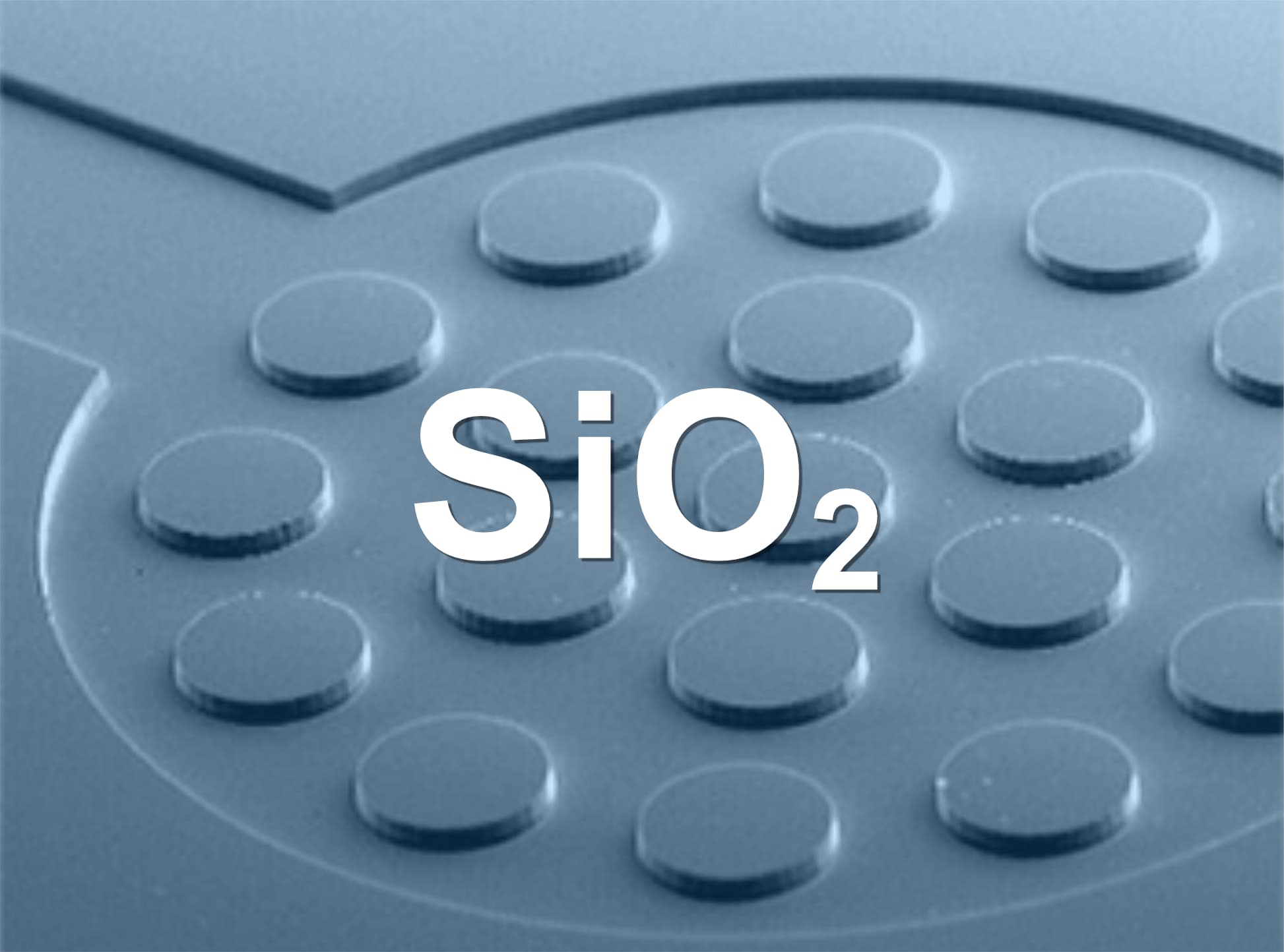
SiO2 Etching
Silicon Dioxide (SiO2) is an oxide of silicon with unique chemical and mechanical properties including excellent abrasion resistance, good electrical insulation and low thermal expansion and high thermal stability.
Button text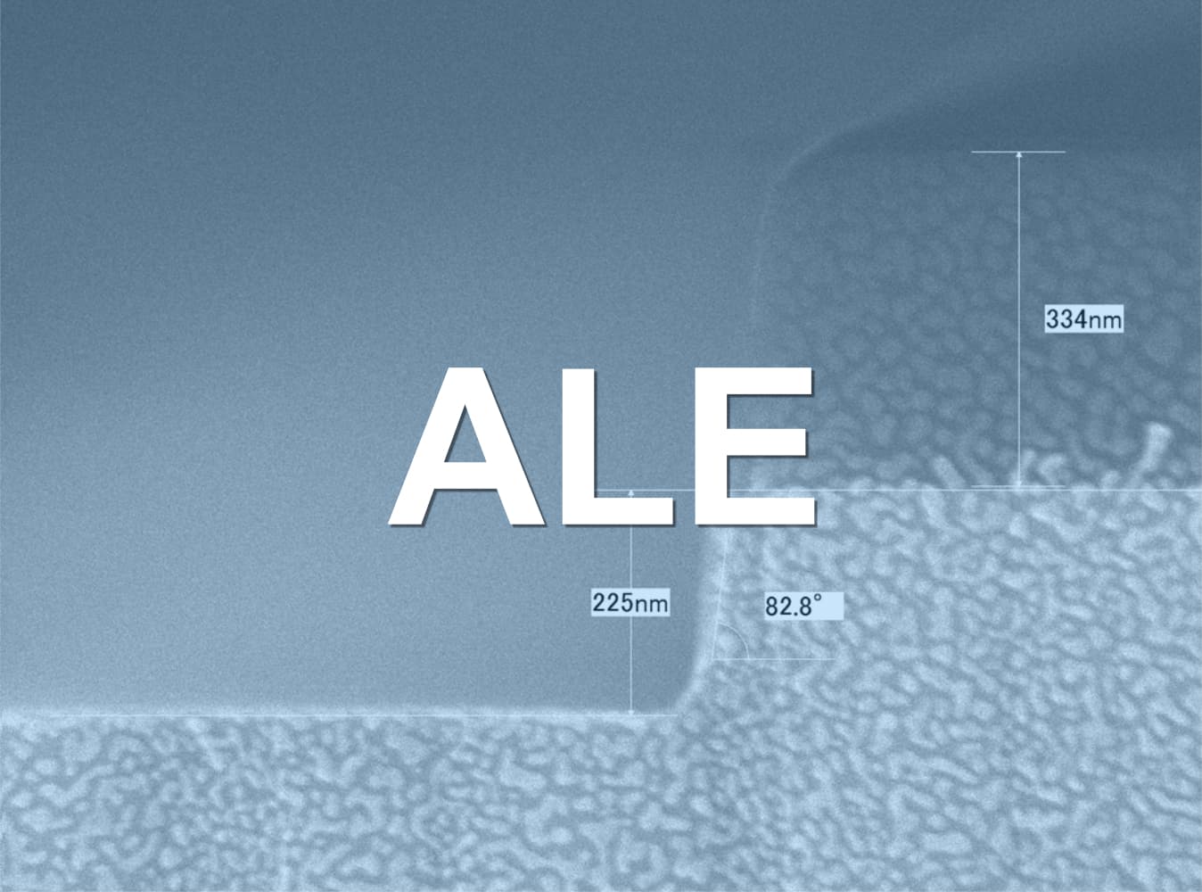
Atomic Layer Etching (ALE)
ALE enables atomic-scale precision for controlled material removal, ensuring uniformity and selectivity in advanced semiconductor fabrication.
Button text