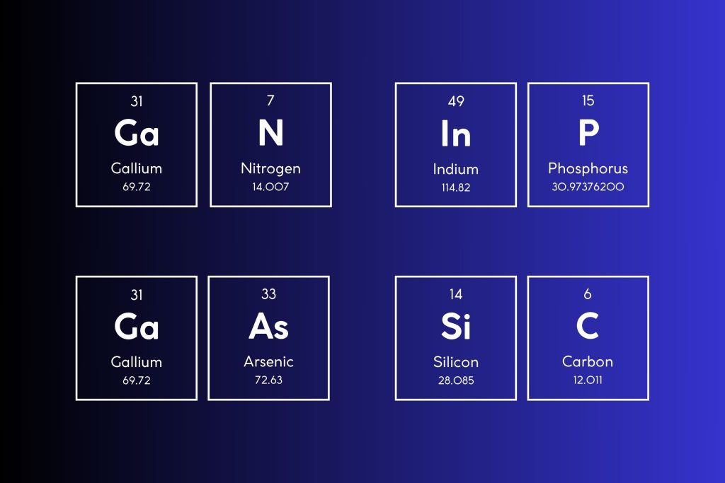
Samco offers high-precision, high-speed processing of III-V compound semiconductors, including GaN, GaAs, InP, and advanced quaternary materials. With a deep foundation in plasma processing technology and decades of industry experience, our etching systems are trusted by customers worldwide for demanding applications, from laser diodes to RF devices and microLED displays.
Designed to address specific III-V material challenges, Samco’s systems combine innovative design elements—such as the Tornado ICP Coil®—with advanced vacuum configurations that optimize etchant species distribution, reduce byproduct redeposition, and ensure stable plasma conditions even at low pressures. Our team works closely with each customer to develop customized etch recipes and optimize process performance, providing not only leading-edge equipment but also robust technical support that adapts to the evolving needs of compound semiconductor fabrication.
Gallium nitride (GaN) etching

Samco has established a strong presence in GaN (gallium nitride) plasma etching for high-performance applications, including laser diodes and LEDs.
With the increasing demand for micro LEDs in advanced displays, Samco is at the forefront of developing specialized GaN etching process technologies. We actively collaborate with international research institutions to refine these processes, advancing the capabilities and precision needed for next-generation display applications.
Damage reduction on AlGaN layer
0
Bias Power, Low Damage Etch
Plasma ashing employs ions and radicals generated in plasma to remove photoresist. This process uses two primary mechanisms:
- Physical sputtering by ion bombardment.
- Chemical reactions forming volatile molecules like H₂O and CO₂.

High etch selectivity of GaN over AlGaN
60:1
Selectivity Rate
Samco solved the selectivity issue by using a small flow of an additive gas (“Gas X”) in a chlorine-based gas plasma mixture. As a result, an etch selectivity of 60:1 (GaN/AlGaN) is achieved, and the etch process is successfully stopped on the AlGaN interface without over-etching. Additionally, the plasma damage on the AlGaN layer is reduced by employing lower RF bias power.


Wide control of the trench shape from vertical to forward tapered processing. We used GaN epitaxially grown on sapphire substrates and etched them with Samco’s RIE-400iP.
Products

For fabrication of GaN-based light emitting devices. We also provide equipment for trench and mesa etching for 4H-SiC power devices.
Products

Samco offers high selectivity etching of GaN/AlGaN for GaN RF device fabrication by ICP plasma etching system.
Products

Light confinement is achieved by making the element end of the LED inverted taper, which improves the intensity of light emission.
Products
Gallium arsenide (GaAs) etching
Samco’s advanced GaAs etching technology ensures superior uniformity across 6-inch wafers, supporting precise device production. Our optional interferometry endpoint detection system guarantees stable and accurate etch stops, even across multiple wafers. The market for Vertical Cavity Surface Emitting Lasers (VCSELs), which utilize GaAs mesa etching, is rapidly expanding. These lasers are integral to various applications, including smartphones and autonomous driving systems. Samco’s GaAs etching solutions are engineered to meet the high demands of these emerging technologies.

By replacing the upper DBR of the active layer with a diffraction grating, it is possible to improve the performance of the VCSEL.
Products

Our process technology enables high-speed vertical machining up to and including ø6 inch wafers. This shows an example of a GaAs mesa etching process with an etching rate of about 2 μm/min.
Products

This shows an example of vertical mesa etching on a ø3 inch VCSEL (Vertical Cavity Surface Emitting Lasers) wafer.
Products

Achieved 3.8 μm deep GaAs etching with <±5% uniformity across ø6-inch wafers, ensuring precise and consistent results for MicroLED fabrication.
Products

The system of semiconductor quantum dots coupled with nano-resonators is expected to be applied to quantum photonics devices and quantum information devices.
Products

Fine anisotropic etching VCSEL (Vertical-Cavity Surface-Emitting Laser) is a semiconductor laser whose resonance direction is perpendicular to the substrate surface.
Products

Products
Indium phosphide (InP) etching

Indium Phosphide (InP) is essential for high-volume and high-speed telecommunications technology. However, controlling the etch profile can be challenging due to unwanted byproduct deposition. Samco offers state-of-the-art InP plasma etching solutions tailored for laser diode fabrication. Our technology precisely controls sidewall angles and surface roughness on both sidewalls and bottoms, ensuring optimal device performance even under high-temperature conditions.

The anisotropic and small footing ridge shape with a width of 1.8 μm and a depth of 2.5 μm has been achieved.
Products

This process can be applied to semiconductor lasers and photonic crystals. A smooth pillar, 0.7 µm in diameter and 4 µm deep, with vertical, no sidewall or bottom roughness, has been formed.
Products
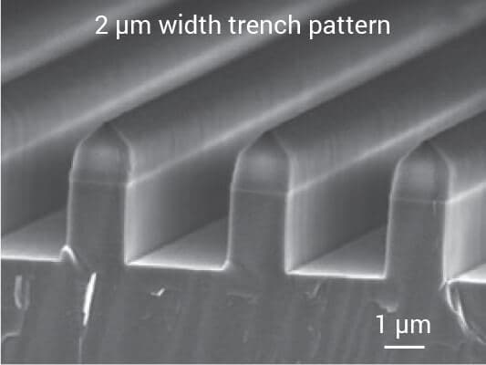
Silicon carbide (SiC) etching
Silicon Carbide (SiC) is renowned for its exceptional electrical breakdown strength and thermal conductivity, making it ideal for high-efficiency power devices in demanding applications like automotive, aerospace, and high-speed electronics. Despite its advantages, SiC presents fabrication challenges, particularly in achieving precise etch profiles and maintaining high etch rates due to its inherent hardness and low etch selectivity.
Samco addresses these challenges with advanced SiC etching solutions designed for trench-type metal-oxide-semiconductor field-effect transistor (MOSFET) fabrication. Our technology ensures smooth sidewalls and high etch rates, achieving up to 775 nm/min, and maintains superior etch selectivity of over 13:1 (SiC/SiO₂). These capabilities support the production of high-reliability SiC power devices, driving innovation and performance in next-generation electronic systems.
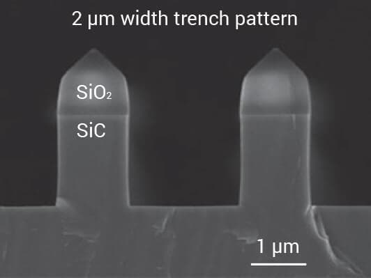
Micro trench-free profile with smooth sidewalls
A 2 μm deep trench profile (2 μm width) is fabricated. With an adjustment of electrode gap and bias power, the micro-trench is removed, and the sidewall shows a smooth surface.
High etch rate
700
nm/min
With an adjustment of the ICP and bias power, an etch rate of over 700 nm/min is achieved.
High etch selectivity over SiO2 mask
13:1
Selectivity rate (SiC/SiO2)
A selectivity of over 13:1 (SiC/SiO2) is possible with pressure optimization.


Trench gate processing of SiC MOSFETs by Samco’s cutting edge ICP etching system. It has smooth sides and a sub-trenchless round shape.

High SiC etch rate of 1.3 μm/min Result of via hole processing for contact from the back side of SiC substrate to electrode by ICP etching system