Samco’s GaAs etching technology provides precise, high-uniformity plasma dry etching essential for fabricating VCSELs, laser diodes, MicroLEDs, RF devices, and photonic structures. Our ICP-RIE systems enable excellent profile control, stable etch performance, and accurate endpoint detection across wafer sizes up to 6 inches.
With decades of experience in III-V etching, Samco supports both production environments and advanced research laboratories worldwide.
Gallium arsenide (GaAs) is a III-V semiconductor with:
These properties make GaAs ideal for:
Our ICP-RIE systems maintain excellent uniformity for GaAs mesa and trench etching. Optional interferometry endpoint detection ensures high-accuracy etch stops even for multi-wafer processes.
Samco’s ICP-RIE systems are optimized for precise GaAs etch profiles, enabling:
These capabilities support the performance demands of modern optoelectronic and RF devices.
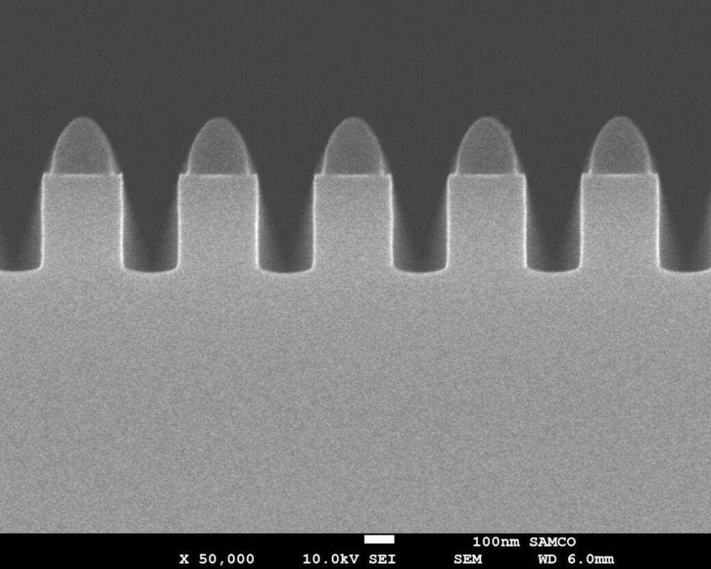
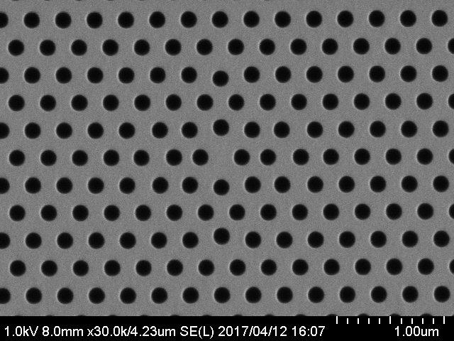
By replacing the upper DBR of the active layer with a diffraction grating, it is possible to improve the performance of the VCSEL.
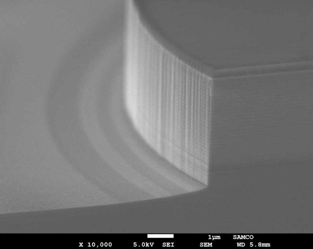
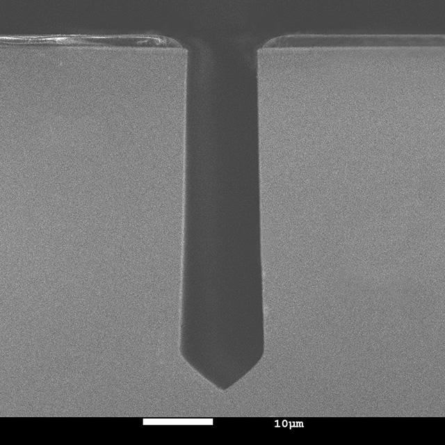
Our process technology enables high-speed vertical machining up to and including ø6 inch wafers. This shows an example of a GaAs mesa etching process with an etching rate of about 2 μm/min.
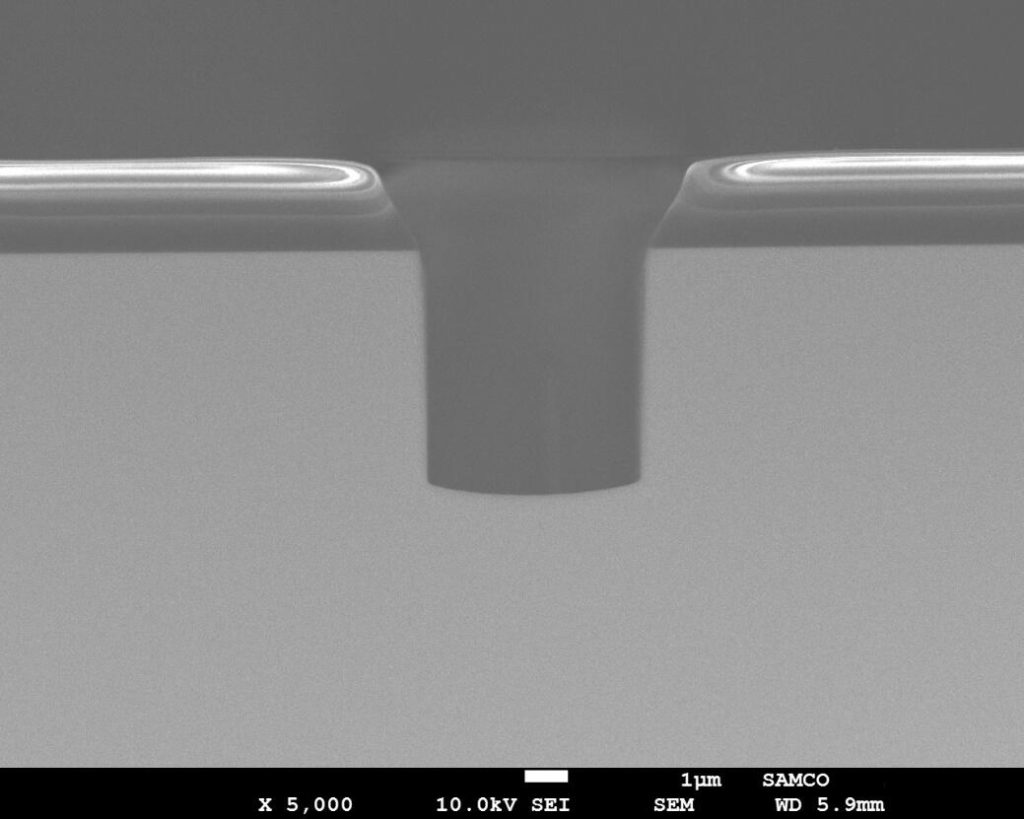
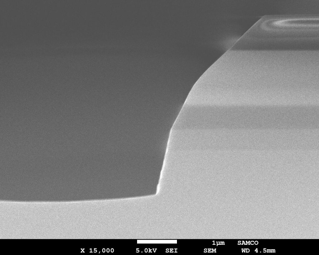
This shows an example of vertical mesa etching on a ø3 inch VCSEL (Vertical Cavity Surface Emitting Lasers) wafer.
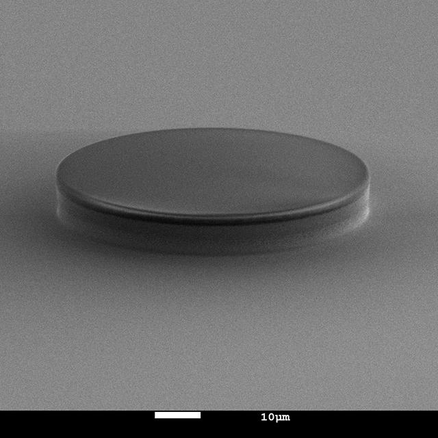
Achieved 3.8 μm deep GaAs etching with <±5% uniformity across ø6-inch wafers, ensuring precise and consistent results for MicroLED fabrication.
The system of semiconductor quantum dots coupled with nano-resonators is expected to be applied to quantum photonics devices and quantum information devices.
Fine anisotropic etching VCSEL (Vertical-Cavity Surface-Emitting Laser) is a semiconductor laser whose resonance direction is perpendicular to the substrate surface.