Stable Device Isolation Processing for 6-Inch GaN-Based Power Devices
GaN device isolation etching using ICP-RIE and endpoint detection enables uniform processing and stable multi-wafer semiconductor production.
Samco’s advanced GaN etching process delivers precise, damage-controlled plasma dry etching for high-quality GaN device fabrication. From power transistors and RF components to microLEDs and laser diodes, Samco systems provide stable plasma control, high selectivity, and finely tunable etch profiles for a wide range of GaN structures.
Built on decades of plasma process expertise, our ICP-RIE systems such as the RIE-400iP and RIE-800iPC enable finely tuned GaN etching performance for next-generation semiconductor and optoelectronic devices.
Gallium Nitride (GaN) is a wide-bandgap III-V semiconductor defined by:
These properties make GaN essential for:
GaN fabrication requires highly controlled plasma processing—especially low-damage etching and precise depth control—both of which are strengths of Samco’s ICP-RIE technology.
Samco’s GaN etching technology supports a wide range of compound semiconductor applications, including LEDs, laser diodes, and GaN-based power devices. Our systems achieve excellent profile control and high selectivity between GaN and AlGaN, while minimizing plasma-induced damage on sensitive device layers.
Key performance features include:
These capabilities support both production environments and advanced R&D applications.
0
Bias Power, Low Damage Etch
Plasma ashing employs ions and radicals generated in plasma to remove photoresist. This process uses two primary mechanisms:

60:1
Selectivity Rate
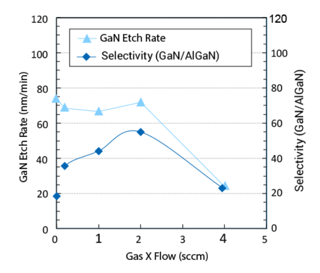
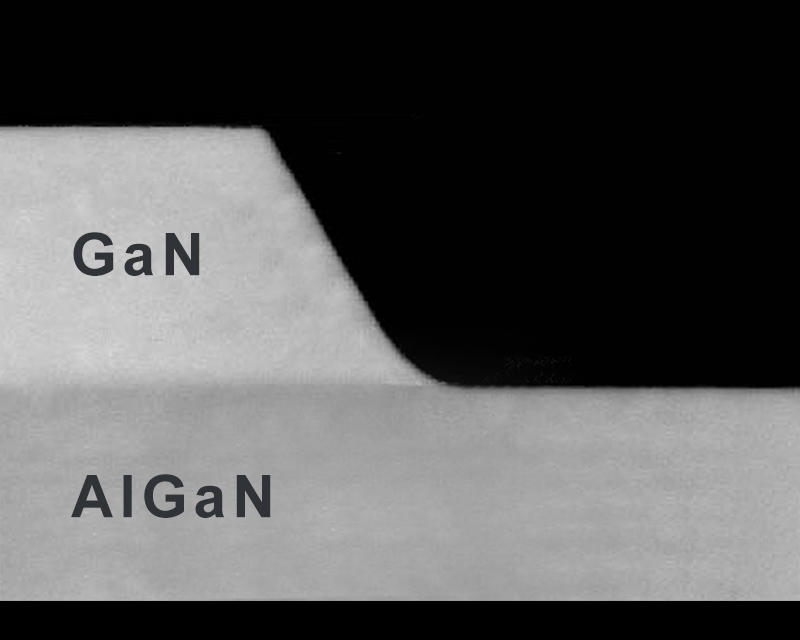
Samco solved the selectivity issue by using a small flow of an additive gas (“Gas X”) in a chlorine-based gas plasma mixture. As a result, an etch selectivity of 60:1 (GaN/AlGaN) is achieved, and the etch process is successfully stopped on the AlGaN interface without over-etching. Additionally, the plasma damage on the AlGaN layer is reduced by employing lower RF bias power.
Properly tuned ICP conditions suppress micro-masking and byproduct redeposition, enabling smooth etched surfaces without skirts, notching, or pillar formation—critical for laser diodes, LEDs, and ELO-based GaN structures.
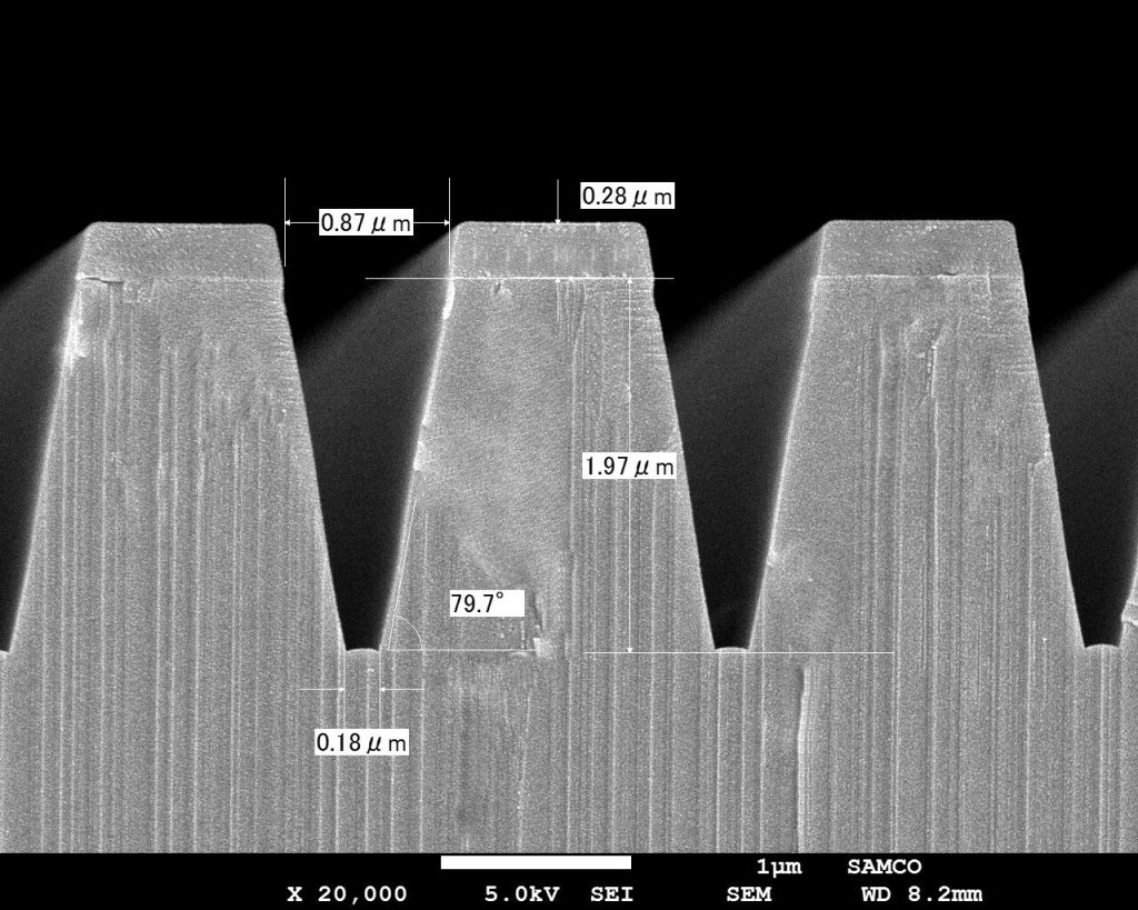
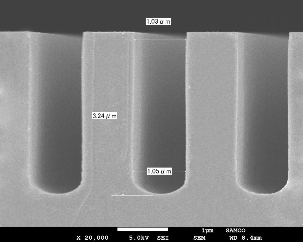
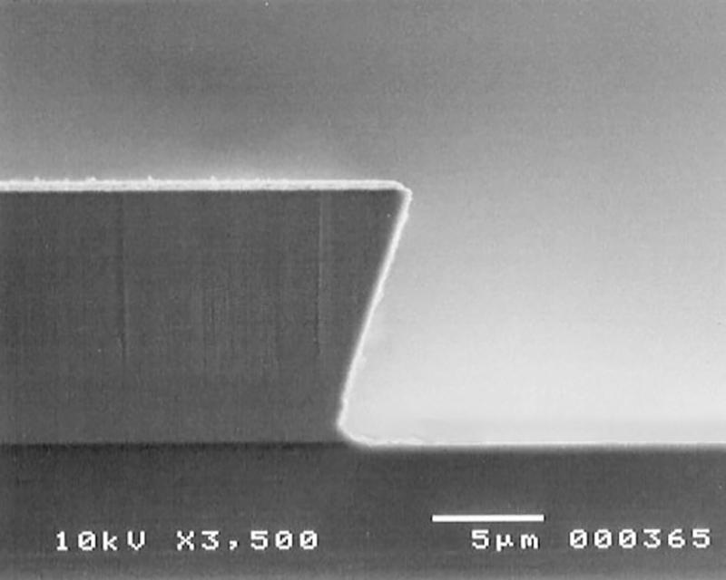
Wide control of the trench shape from vertical to forward tapered processing. We used GaN epitaxially grown on sapphire substrates and etched them with Samco’s RIE-400iP.
For fabrication of GaN-based light emitting devices. We also provide equipment for trench and mesa etching for 4H-SiC power devices.
Samco offers high selectivity etching of GaN/AlGaN for GaN RF device fabrication by ICP plasma etching system.
Light confinement is achieved by making the element end of the LED inverted taper, which improves the intensity of light emission.

GaN device isolation etching using ICP-RIE and endpoint detection enables uniform processing and stable multi-wafer semiconductor production.
Key etching challenges in AlGaN/GaN power device fabrication and solutions for precise plasma etching of GaN-based semiconductor structures.