As one of the most promising materials in compound semiconductors, Gallium Nitride (GaN) demonstrates high electron mobility and a wide bandgap, enabling numerous next-generation applications. GaN-based devices, from High Brightness LEDs in consumer electronics to emerging power devices, are central to advancements in displays, lighting, and high-performance power systems. The unique AlGaN/GaN heterointerface generates a high-concentration two-dimensional electron gas (2DEG) with impressive mobility (1500 cm²/Vs), offering GaN devices significant advantages over silicon in breakdown voltage, switching speeds, and resistance. Due to these benefits, GaN power devices are becoming increasingly critical in power generation, rail systems, and electric vehicle technology.
Challenges in GaN Power Device Fabrication
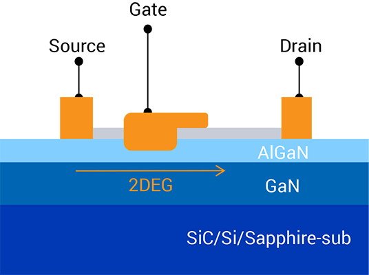
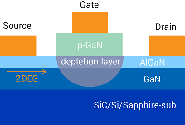
Achieving precise control in GaN power device fabrication presents key challenges, particularly in “normally off” configurations, which are preferred for safety. While AlGaN/GaN High Electron Mobility Transistor (HEMT) devices naturally default to an “on” state, research into planar gate and camel gate structures is ongoing to achieve a “normally off” operation. Below are some of the primary etching challenges in AlGaN/GaN fabrication:
- Offset Time in AlGaN Recess Etching:
The native oxide layer on AlGaN can prevent effective etching, leading to a delay (offset) time of up to 120 seconds. Increased RF power may reduce this offset, but it risks damage to the AlGaN layer, making reproducibility and thickness control difficult. - Precise Thickness Control of AlGaN Layers:
Thickness control is essential for achieving optimal Vg-Id characteristics in recessed-gate structures, directly impacting device performance. Minor deviations in AlGaN layer thickness can lead to increased drain current and reliability concerns. - Gate Leakage from Plasma Damage:
Plasma damage, particularly during silicon nitride (SiN) passivation etching, can cause gate leakage, deteriorating the performance of the AlGaN/GaN device. Minimizing plasma exposure while maintaining precision is crucial to preserving device integrity. - Etch Selectivity Between GaN and AlGaN Layers:
Ensuring high etch selectivity for GaN over AlGaN is essential, especially during the etching of p-GaN layers. Over-etching can damage underlying AlGaN, affecting sheet resistance and device longevity.
These challenges underscore the need for optimized etch processes and precise control at each step. As GaN power devices continue to evolve, overcoming these hurdles in AlGaN/GaN etching will be essential to unlocking their full potential across various high-performance applications.
Samco Solutions for AlGaN/GaN Power Device Etching
Samco’s expertise in compound semiconductor etching positions us as a leader in addressing these challenges. With advanced plasma etching technology and customizable system configurations, our etching solutions support the high precision, control, and repeatability needed for complex AlGaN/GaN structures. We provide robust process recipes tailored to each customer’s unique requirements, enhancing device performance, yield, and reliability across a range of GaN-based power applications.