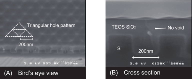
Photo courtesy of Professor Nobuhiko Nishiyama, Tokyo Institute of Technology.

Since its inception as a manufacturer of plasma-enhanced chemical vapor deposition (PECVD) equipment, Samco has been providing enabling PECVD process and hardware technologies to the market. In addition to the commonly used silane gas chemistry, Samco has developed liquid source CVD™ technology that utilizes liquid precursors that are safe and easy to use for the deposition of silicon nitride and silicon oxide thin films. Furthermore, Samco has developed a unique cathode-coupled PECVD system configuration whereby a radio frequency (RF) is applied to the lower/substrate electrode and ionic species are involved in depositing a high-density and conformal film at a rapid rate. The cathode-coupled PECVD has been widely adopted by manufacturers of optical waveguide and RF filter devices. This report introduces the new cathode-coupled PECVD system, PD-200STL, which allows switching of the RF driven electrode to be either the upper electrode (anode-coupled) or the lower/substrate electrode (cathode-coupled).
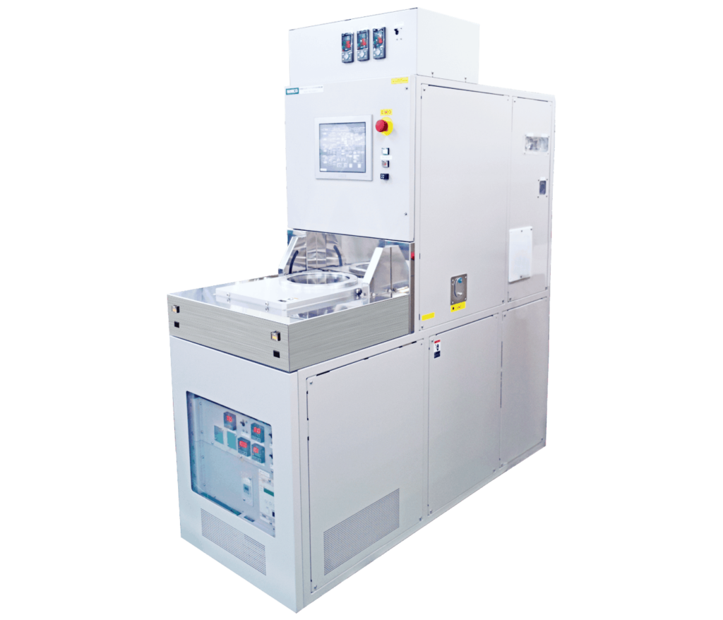
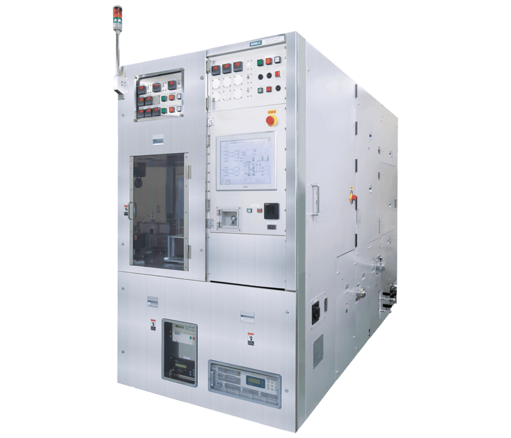
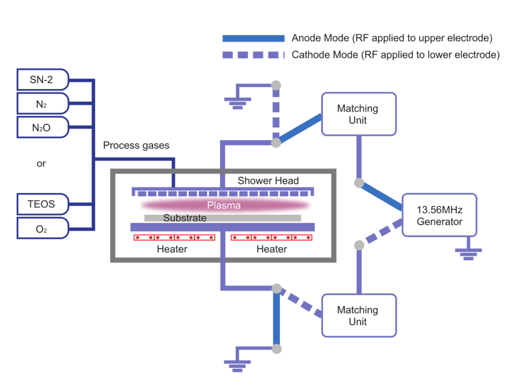
The PD-200STL (Figure 1) is equipped with one matching unit that is connected to the upper electrode and another one connected to the lower/substrate electrode that facilitates the switching of the RF power connection to either electrode turning it to be either hot or ground (Figure 2). This enables the selection of either an anode or cathode coupled processing mode to meet different film property requirements. Switching of the RF driven electrode can be conveniently programmed in the process recipe using the system touch display without necessitating any manual hardware changes.
The PD-200STL is equipped with a ø220 mm carrier tray that supports wafer sizes ranging from small pieces to 8″. The substrate heater temperature can be controlled from ambient temperature to 400°C. Samco has consolidated its expertise in the anode and cathode coupled PECVD processes, which enables the PD-200STL to deposit films with tunable properties.
| Process | Hardware Configuration | Process Chemistry | |
| 1 | Void-free gap-filled SiO2 | Cathode-coupled | TEOS, O2, Ar |
| 2 | Low temperature SiO2 film deposition | Cathode-coupled | TEOS, O2 |
| 3 | Refractive Index control of SiON film | Anode-coupled | SN-2 (Liquid precursor), N2O, N2 |
Using the PD-200STL, it is possible to fill triangular hole patterns with approximately 200 nm width without voids. Using solely the cathode-coupled PECVD technique, the film is selectively deposited on the side of the pattern apertures, thereby closing the apertures prior to the filling of the holes, resulting in the formation of voids. However, if the cathode-coupled PECVD process is augmented by the Ar sputtering/etch-back process, the two alternating processes can achieve void-free gap-filling, even with pattern width that is close to 200 nm (Figure 3).
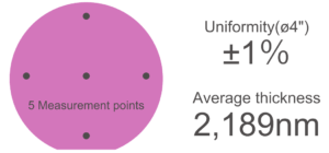
Secondly, we have demonstrated deposition of silicon oxide film at low temperatures using the cathode-coupled configuration. 2 µm thick silicon oxide film was deposited on a ø4″ silicon wafer at a substrate heater temperature of 80°C. Despite the film thickness, no cracks were observed in the film. Furthermore, deposition thickness uniformity of 1% was obtained using a 5-point measurement (Figure 4).
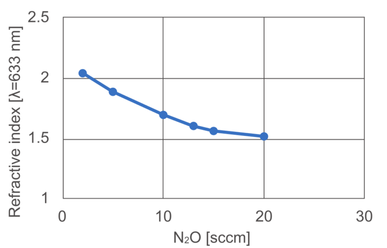
Finally, Figure 5 illustrates the refractive index fitting of silicon oxynitride (SiON) film deposited using N2O to SiH4 precursor ratio in the anode coupled configuration. By adjusting the N2O flow rate, the refractive index from 1.514 to 2.003 (λ 633 nm) was achieved.
Three sets of deposition data obtained on the PD-200STL have been presented above. The PD-200STL is an extremely versatile system that allows for a diverse range of deposition conditions by utilizing both the anode coupled and cathode coupled configurations.
The PECVD system PD-200STL is equipped with an anode/cathode switching function that allows for a wide range of film deposition conditions possible, thereby providing differentiation and versatility to support broad research and development requirements.
Samco wishes to express our gratitude to Professor Nishiyama of Tokyo Institute of Technology who granted permission to share the SEM images in this report.