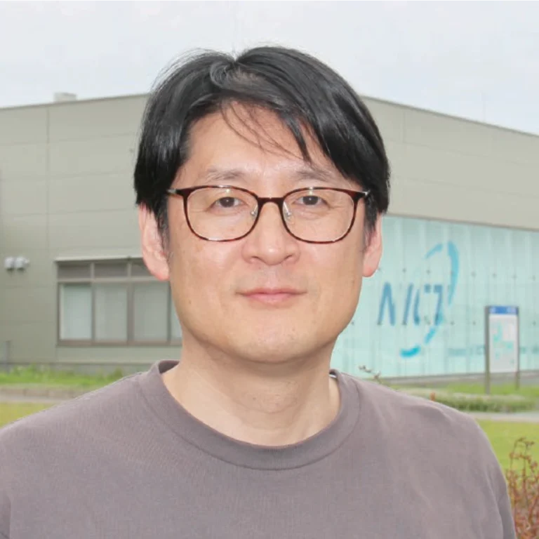
Shigehito Miki, Ph.D.
Deputy Director, Advanced ICT Device R&D Promotion Center, National Institute of Information and Communications Technology, Kobe Frontier Research Center, Advanced ICT Research Institute
For this interview, we visited the Kobe Frontier Research Center of the Advanced ICT Research Institute at the National Institute of Information and Communications Technology (NICT) to speak with Dr. Shigehito Miki about his research on superconducting nanostrip single-photon detectors (SNSPDs).
Education
Apr. 2000–Mar. 2003
Doctoral Program, Graduate School of Science and Technology, Kobe University
Career History
Apr. 2003–Sep. 2005
Researcher, Core Research for Evolutional Science and Technology (CREST), Japan Science and Technology Agency (JST)
Oct. 2005–Sep. 2007
Researcher, National Institute of Information and Communications Technology (NICT)
Oct. 2007–Mar. 2015
Senior Researcher, NICT
Apr. 2015–Mar. 2023
Senior Researcher, NICT
April 2023–Present:
Director, Superconductive ICT Device Laboratory, NICT
April 2026–Present:
Deputy Director, Advanced ICT Device R&D Promotion Center, NICT
Could you tell us about your current research?
At the Superconductive ICT Device Laboratory, we are working to develop electronic and optical devices that use superconducting films and junctions to contribute to future information and communications applications. Within this field, my research focuses on superconducting nanostrip single-photon detectors (SNSPDs), which can detect individual photons—the smallest units of light—with extremely high sensitivity.
Specifically, we process extremely thin superconducting niobium titanium nitride (NbTiN) films, only a few nanometers thick, to form structures known as nanostrips with strip widths of 100 nanometers (nm) or less. When a single photon enters the detector, the superconducting state is locally disrupted, temporarily generating electrical resistance. By reading this change as an electrical signal, the detector can identify individual photons.
SNSPDs are now being actively studied around the world. In quantum information communication and quantum computing, they have become an indispensable key technology. They are also expected to support a wide range of next-generation applications, including LiDAR, deep-space optical communications, and observation of extremely weak light emitted by cells. Although various photon detection technologies exist, SNSPDs are regarded as the world’s highest-performing detectors for single-photon detection in the 1550 nm telecommunication wavelength band, particularly in terms of detection efficiency, low dark count rate, and timing resolution.

Since joining NICT, I have focused on building SNSPD technology from the ground up, at a time when the concept had just been proposed and only a handful of studies had been published. I started to develop the practical systems that can actually be used by researchers and engineers in advanced application fields, including quantum information communication.
To operate an SNSPD, it must be cooled to cryogenic temperatures, specifically around -270°C. This requirement can become a barrier for users. To address this issue, we developed an SNSPD system using mechanical cryocooler which does not require any liquid cryogen, creating a versatile system that users can operate without needing to be conscious of cryogenic cooling.
Today, these systems are used not only in quantum communication and quantum computing research, but also across a variety of other fields, where they serve as important tools supporting daily research and development. In advanced fields that deal with photons, it is no exaggeration to say that the performance of the photon detector can determine the success or failure of the research. By using the detection systems we have developed, researchers can pursue new areas of technology development that were previously impossible. I feel that our work is helping to push forward the frontiers of research worldwide.
What led you to this field of research, and how did your career develop?
Looking back, this began quite a long time ago. As a student I belonged to the Department of Computer Science and Systems Engineering in the Faculty of Engineering at Kobe University, where I mainly studied information processing and programming. The turning point came when I was assigned to a laboratory in my fourth year of university.
At that time, my academic supervisor was studying microwave wireless power transmission and was conducting joint research with researchers at NICT. Through that connection, I first visited what was then NICT’s superconductivity research lab in 1998, while I was still a student. That visit became the starting point for my involvement in superconducting device research.
It was very different from the field I had studied up to that point, but I was strongly attracted to the opportunity to conduct world-class research at a national research institute. I was then given the opportunity to conduct research at NICT as a trainee. During my doctoral program, I followed a somewhat unusual path: through Kobe University’s cooperative graduate school system, I carried out my research at NICT and obtained my doctoral degree.
After receiving my Ph.D., I worked for about two and a half years as a researcher in the Core Research for Evolutional Science and Technology (CREST) program of the Japan Science and Technology Agency (JST), conducting device research at what was then Osaka Prefecture University, now Osaka Metropolitan University. There as well, I worked with superconducting materials, although the devices had functions somewhat different from those I study today.
Around 2001, the basic principle of the single photon detector now known as the SNSPD was proposed for the first time by an overseas research institute. At the time, the technology was still in its earliest stages worldwide. As I read the first papers that began to appear, I felt a strong impulse: “This looks fascinating. I want to try turning this new device into a reality myself.”
When I considered where in Japan would be best suited for research on this single photon detector, the answer I arrived at was the very superconductive electronics laboratory where I had previously worked. The reason was that the laboratory already had the thin-film deposition technology needed for SNSPDs, namely the ability to form high-quality superconducting NbTiN films only a few nanometers thick. In addition, the cleanroom was already equipped with facilities capable of nanometer-scale microfabrication, including Samco equipment.
When I told the laboratory director at the time that I wanted to launch new research on SNSPDs, it turned out that he also happened to be interested in SNSPDs and had been thinking of starting research in this area. When I joined NICT as a staff member in October 2005, SNSPD research had not yet been established there. As the first person in charge, I built the research effort literally from scratch, from optimizing NbTiN thin films to establishing the fabrication process and assembling the complete system that operates at cryogenic temperatures.
What are your thoughts on the future of this research field?
SNSPDs, which are single photon detection devices based on superconducting nanostrips, have come very close to an ideal state in terms of performance. Detection efficiency has exceeded 95%, approaching nearly 100%. Noise that causes false signals, known as dark counts, has also been reduced to extremely low levels. Some mature technologies have already been transferred for practical use. At the same time, as the technology advances, new demands are emerging.
In current SNSPD systems, the number of detectors that can be installed and cooled inside a mechanical cryocooler is typically only a few, or at most around ten. However, with the development of quantum technologies, I believe future systems will require hundreds, thousands, or even more detectors. A new challenge is how to integrate as many detectors as possible at high density within the limited cooling capacity of a cryocooler.
We are also studying applications such as two-dimensional imaging sensors with ultra-high sensitivity at the single-photon level—in other words, single-photon imaging cameras—by arranging large numbers of detectors in a two-dimensional lattice.
As a recent important result toward realizing highly mass-producible photon detectors, our laboratory demonstrated for the first time in the world that high-performance single-photon detection is possible even when the strip width is greatly increased. Conventionally, fabricating high-performance SNSPDs required extremely narrow nanostrip processing with line widths of 100 nm or less. The advanced and time-consuming nanofabrication process using electron-beam lithography was a major challenge for mass production and large-area fabrication.
In this work, we developed technology to achieve high-performance photon detection without narrowing the strips down to the nanometer scale. We succeeded in detecting single photons with nearly equivalent performance even when the strip width was expanded to approximately 20 μm, more than 200 times wider than conventional structures.
By increasing the strip width to the micrometer scale, it becomes possible to use conventional photolithography instead of electron-beam lithography. This is expected to enable lower-cost, highly mass-producible manufacturing of high-performance photon detectors. We believe this represents a major step toward realizing the large-scale photon detection systems that will likely be required for quantum computing and quantum communication.
You’ve used several of Samco’s systems in your lab. Could you share your experience?

Our devices are fabricated by precisely etching NbTiN thin films only a few nanometers thick, using nanostrip patterns with widths of 100 nm or less formed by electron-beam lithography as masks. Because it is difficult to secure sufficient thickness with electron-beam resist, etching requires a high selectivity and precise shape control.
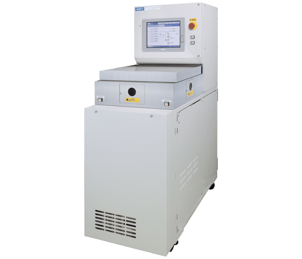
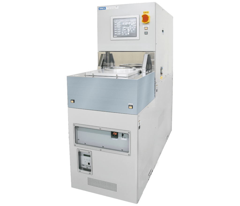
Samco’s RIE-10N and two RIE-10NR RIE systems demonstrate excellent stability and reproducibility in the processing of these delicate superconducting thin films. We also fabricate structures on the nanostrips to collect light. For one of these structures, we deposit SiO₂ films using the PD-220NL plasma CVD system.
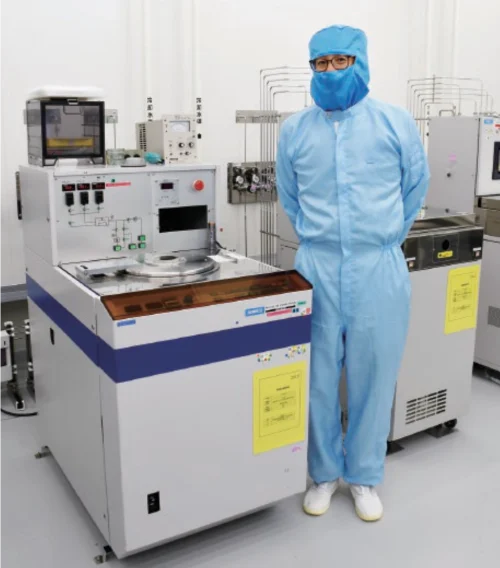
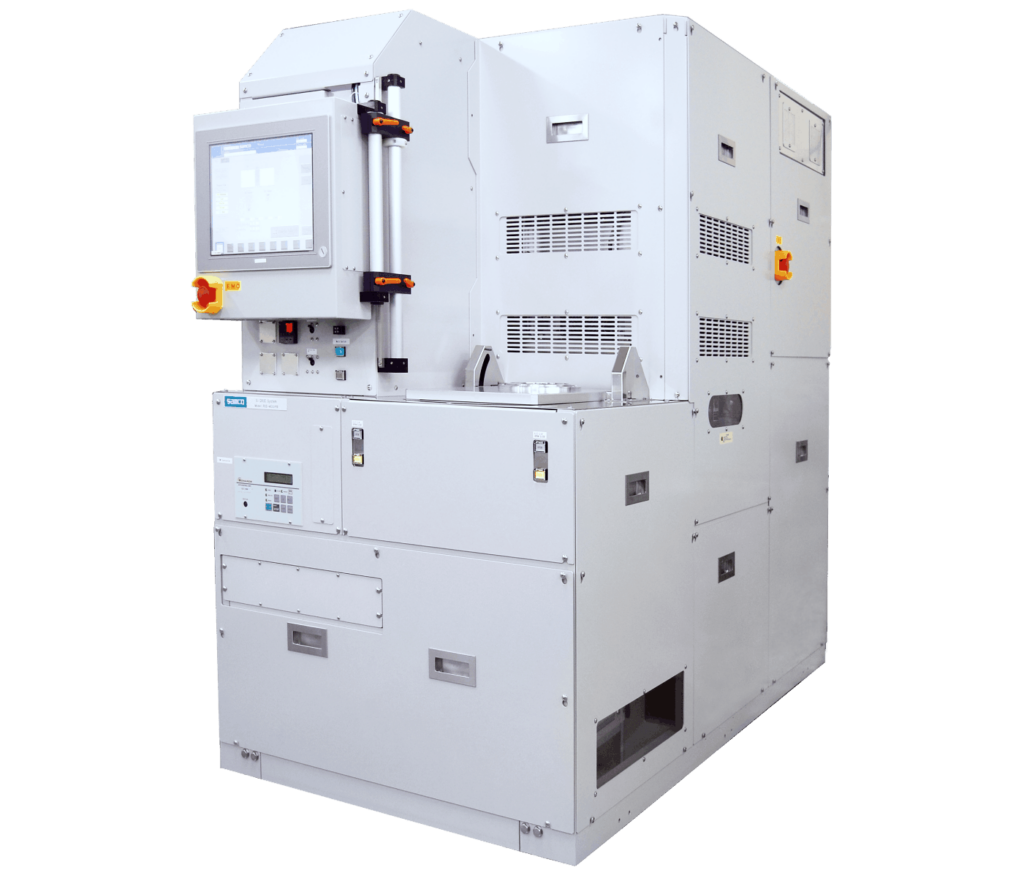
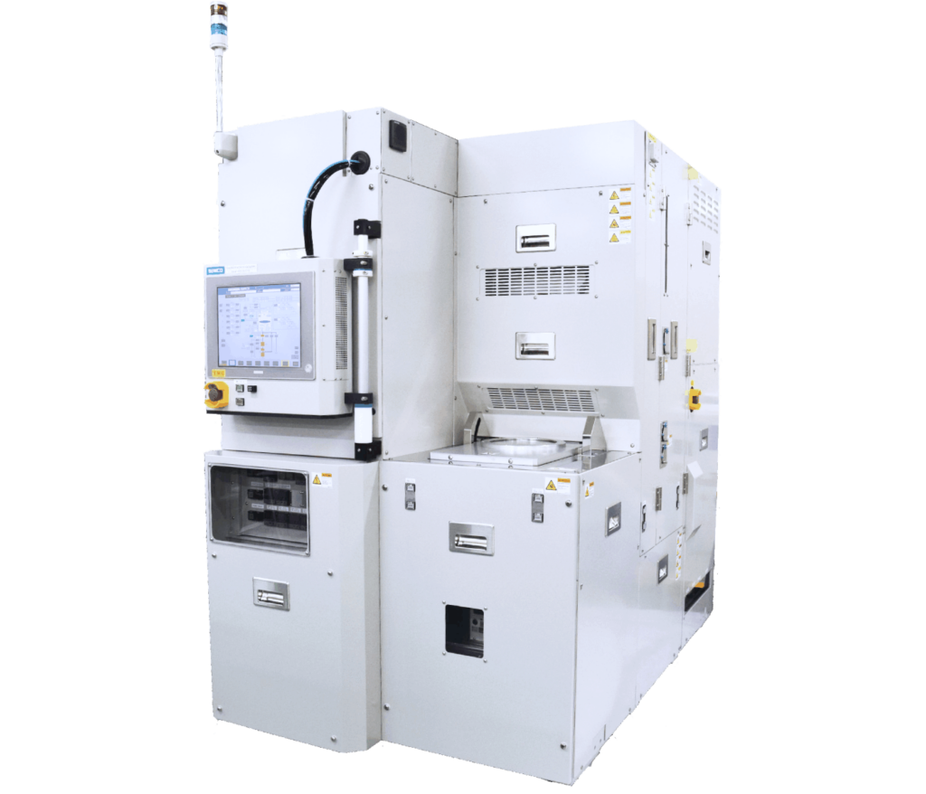
In addition, we use the RIE-400iP ICP etching system for fine processing of silicon to form optical waveguides combined with SNSPDs, and the RIE-800iPB high-speed silicon deep etching system to form MEMS structures. The RIE-10N has continued operating for more than 30 years, which makes us deeply impressed by the robustness of the system and gives us great confidence in its reliability.
What do you keep in mind in your research?
Each researcher has their own style and philosophy, and there is no single correct answer. In my own research, what I try to keep in mind is the attitude of deliberately questioning my own hypotheses and even the successes in front of me.
When advancing research, I value stepping back and asking, “Is this really true?” By verifying results from many different angles and experimentally eliminating possible objections and sources of error one by one, I believe the results that remain can ultimately be proven more convincingly.
How do you spend your days off?
I am not especially fond of crowds or busy urban areas, so in my private time I value spending time in quiet suburbs or natural surroundings with plenty of greenery. On weekends, I often relax at home by watching movies.
My main hobby is skiing, which I have enjoyed since my student days. In winter, I travel with my family to places such as Nagano Prefecture. I am the type of person who tends to think about research even on days off, so I try to consciously switch my mindset through skiing, movies, and similar activities.
Do you have any final thoughts?

As shown by the example of equipment that has continued operating for more than 30 years, I have great trust in Samco as an outstanding semiconductor manufacturing equipment manufacturer whose highly robust systems support Japanese manufacturing.
We are currently working to establish the Kobe Device Collaborative Creation Building, where we are introducing many microfabrication and film deposition systems, including Samco ICP etching and ALD systems. At this facility, we hope to create a place where state-of-the-art equipment can be widely opened to universities and companies, supporting human resource development and process verification for product development.
In addition to developing advanced equipment, I hope Samco will continue to be a partner that supports the future of device development in Japan through technical support and solution proposals.
Thank you for taking the time to speak with us despite your busy schedule.
Interview conducted: May 27, 2026
What are SNSPDs?
Superconducting nanostrip single-photon detectors (SNSPDs) are devices that detect individual photons by monitoring tiny electrical signals generated when light strikes an extremely narrow superconducting nanostrip cooled to cryogenic temperatures. In an SNSPD, a current is applied to the nanostrip at a level close to the maximum it can carry while maintaining its superconducting state. When a photon is absorbed, its energy temporarily disrupts superconductivity in a small region of the nanostrip, creating a localized resistive area known as a hotspot. The formation of this hotspot generates a brief voltage pulse that appears in the readout circuit. By detecting this pulse, the arrival of a single photon can be identified. After detection, the hotspot rapidly cools, and the nanostrip returns to its superconducting state, allowing the detector to be used repeatedly.
SNSPDs offer exceptionally high detection efficiency, extremely low dark count rates, and excellent timing resolution. As a result, they are widely used in fields such as quantum communication, quantum optics, and photon-counting applications.