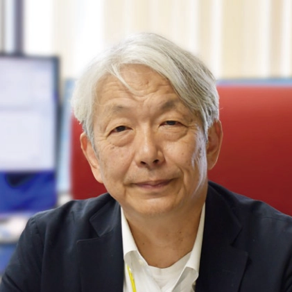
Professor Yasuyuki Miyamoto
School of Engineering, Department of Electrical and Electronic Engineering, Institute of Science Tokyo
For this interview, we visited the Ookayama Campus of Institute of Science Tokyo to speak with Professor Yasuyuki Miyamoto about his research on compound semiconductor-based electronic devices.
Brief History
1988–1992
Assistant Professor, Faculty of Engineering, Tokyo Institute of Technology
1992–2007
Associate Professor, Faculty of Engineering and Graduate School of Science and Engineering, Tokyo Institute of Technology
2007–2013
Associate Professor, Graduate School of Science and Engineering, Tokyo Institute of Technology
2013–2016
Professor, Graduate School of Science and Engineering, Tokyo Institute of Technology
2016–2024
Professor, School of Engineering, Tokyo Institute of Technology
2024–Present
Professor, School of Engineering, Institute of Science Tokyo
Could you tell us about your current research?
My lab focuses on electronic devices using compound semiconductors, especially transistors. We work with two main types of materials: indium phosphide (InP)-based and nitride-based semiconductors.
InP-based materials were originally developed for semiconductor lasers used in optical fiber communication. Today, however, they’re known for enabling extremely fast electronic devices—especially heterojunction bipolar transistors, or HBTs—which currently offer the fastest performance in the world. Nitride semiconductors, on the other hand, are widely recognized for their use in blue LEDs, but they’re also drawing attention as power devices for applications like energy conversion. For example, gallium nitride (GaN) is now common in 65-watt-class AC adapters.
While we previously explored integrating compound semiconductors into silicon transistor channels, shifts in the technology roadmap led us to focus more directly on compound semiconductor devices themselves. Right now, we’re especially interested in pushing the limits of InP- and nitride-based transistor performance.
What led you to this field of research?
In university, I entered the field of electronic and physical engineering. Back in high school, I was into amateur radio and originally wanted to pursue circuits. But I had a friend who was incredibly talented in that area—so talented, in fact, that I thought I might never catch up. That made me reconsider my path.
I realized semiconductors were something you couldn’t explore as a hobby—they required the resources of a university or research institution. That’s what drew me in. I joined a semiconductor lab and started out studying semiconductor lasers, learning about crystal growth and wet etching.
When I completed my PhD, I was encouraged to remain in the lab, and at the time, I fully intended to continue my research on semiconductor lasers. However, Professor Yasuharu Suematsu suggested that I shift my focus to electronic devices. Under his guidance, and working alongside Professor Kazuhito Furuya, I began researching electronic devices during my time as an assistant professor.
In some ways, I simply followed the natural course of events—but that path led me into this field, where I’ve remained ever since. I’ve been working with indium phosphide (InP) since my fourth year as an undergraduate, which means I’ve been using this material for over 40 years. Back then, InP was already recognized as an ideal material for semiconductor lasers operating at 1.3 µm and 1.5 µm—wavelengths critical for fiber-optic communications. Even today, InP continues to be the material of choice for optical communication applications.
What are your thoughts on the future of this research field?
Now that I’m 64, I find myself thinking more about the future of the field as a whole rather than just my own work.
There’s a growing sense that InP-based devices—especially HBTs—will be essential in the years to come. That’s because InP still enables the world’s fastest transistors. The performance of high-frequency devices is usually measured by two values: the transition frequency (fT), where current gain becomes one, and the maximum oscillation frequency (fmax), where power gain becomes one. InP devices currently hold the highest records for both.
The volume of communication data is increasing explosively. Optical fiber networks now require even faster data transmission, and to send more information over a single wavelength, we’re pushing signal frequencies beyond 200 Gbaud. Silicon-based transistors can’t keep up at these speeds—this is where InP-based devices, especially HBTs, are stepping in.
These high-speed transistors are crucial for backbone communication networks—linking cities like Tokyo and Osaka, or even crossing continents. As wireless communication systems like 5G and 6G expand, the need for faster wired infrastructure becomes even more pressing. InP HBTs are a strong candidate to fill that role.
There was a time when many Japanese companies were actively researching InP devices, but interest tapered off. Now, only a few organizations in Japan are still working in this field. That said, I believe InP HBTs have the potential to become indispensable for the future of high-speed communications.
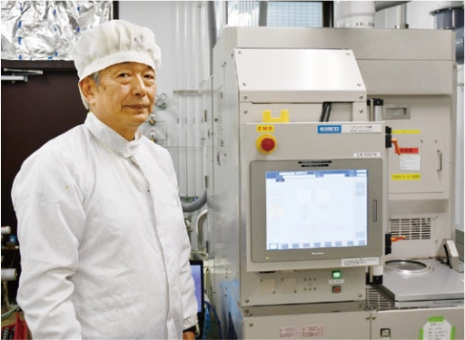
You’ve used several of Samco’s systems in your lab. Could you share your experience?
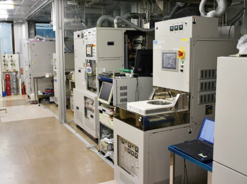
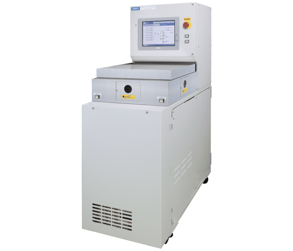
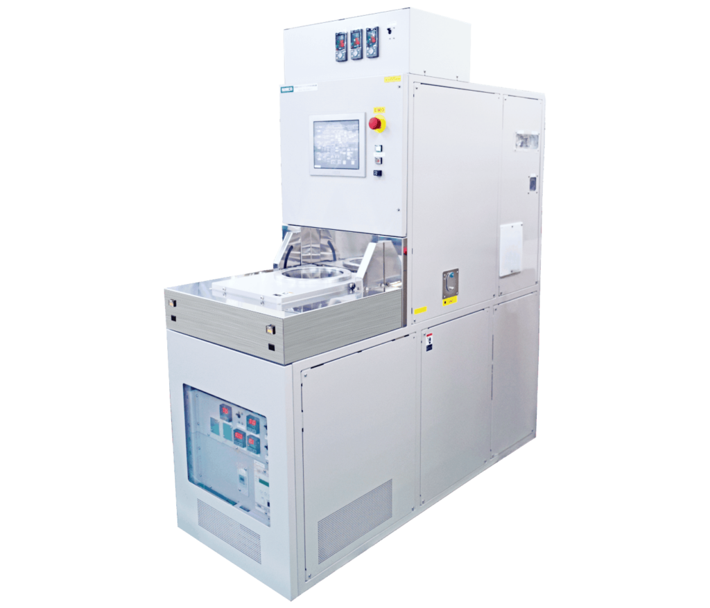
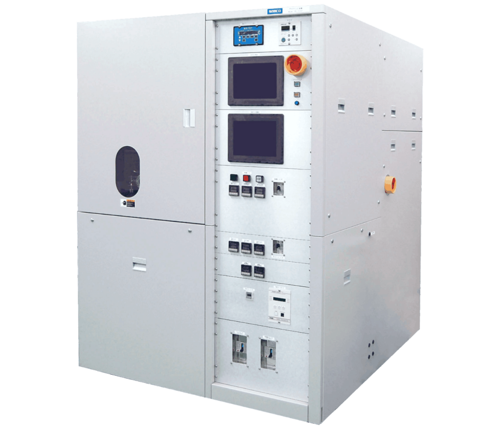
Anode/cathode switching plasma CVD system ‘PD-200STL’
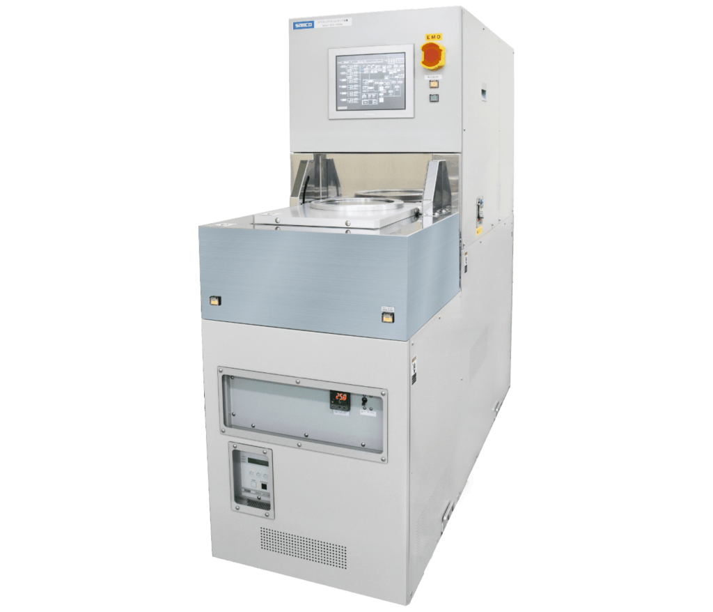
ICP etching system ‘RIE-101iPH’
Parallel plate dry etching systems ‘RIE-10NR’, ‘RIE-10NRN’
Liquid source CVD system ‘PD-100ST’.
One of the most memorable systems for me is the RIE-10NR dry etching system. Before that, we had to manually operate each valve one at a time. But with the RIE-10NR, we could process wafers simply by pressing a button on the touchscreen. That shift to recipe-based automation was groundbreaking for us.
The system’s reproducibility is excellent, too—we now own three RIE-10NR units and use them regularly. They’re reliable and user-friendly.
Another workhorse in our lab is the plasma CVD system compatible with liquid precursors. We use TEOS (tetraethoxysilane) as a silicon dioxide source. Compared to SiH₄ (silane), which is flammable and requires strict gas safety training, TEOS is much easier and safer to handle. That’s a significant benefit.
Our current CVD system, the PD-200STL, replaced an older PD-240 model. We mainly use it for SiO₂ deposition. Thanks to the stable operation of these systems, we’re able to focus fully on developing new devices. In a university research setting, tools that are both easy to use and capable of consistent processing performance are incredibly valuable.
I’d also like to touch on equipment sharing in academia. Devices purchased with grants or national project funding are technically project-specific. But it’s impractical to buy expensive tools for each individual project. About 20 years ago, the Ministry of Education, Culture, Sports, Science and Technology (MEXT) introduced a system for shared equipment usage, which evolved into today’s ARIM (Advanced Research Infrastructure for Materials) program.
This system allows us to share equipment across labs by collecting user fees. That way, we can pool resources for maintenance and supplies, and everyone can access essential tools. Samco systems play a major role in this—especially plasma enhanced CVD and dry etching equipment, which are mainstays in many compound semiconductor research labs.
What do you emphasize in your daily research?
What matters most to me is doing something that excites me. I feel the most joy when I come up with a new idea and it works—whether that’s in an experiment, a simulation, or gaining a new insight.
I tell my students that it’s hard to generate ideas at the beginning. You need to gain hands-on experience and understand the basics first. In the first six months, it’s okay if you don’t know what’s going on—just follow instructions and observe. As you build experience, you start asking questions, testing ideas, and saying, “What if I try this?”
When something finally works, that’s the most rewarding moment. Of course, ideas need to be feasible—you have to understand what’s technically possible. But when students bring unique ideas to the table and we try them together, it’s exciting. And if it succeeds, it becomes a huge confidence boost for them.
How do you like to spend your free time?
My hobby is water polo. I’ve been playing since my first year of high school—almost 50 years now. I’m also the faculty advisor for the university swim team.
I try to practice whenever I can. I don’t play every weekend, but I swim about twice a week. Just the other day, I swam 1.2 kilometers in the evening.
Water polo is a physically demanding sport. You need stamina to keep up with your opponents, whether you’re on offense or defense. Of course, ball handling is important, but in the end, it’s all about swimming power. I’ll be competing in the World Masters Games in Taiwan next month as part of a 50+ age group team. It’s a great way to stay healthy.
Do you have any final thoughts?
I believe the introduction of automated systems like Samco’s plasma CVD systems and dry etching tools has fundamentally changed how semiconductor research is conducted in Japanese universities.
Older tools were simpler in design, and while that made them easy to repair yourself, it also meant taking full responsibility for operation and maintenance. Today’s systems are far more sophisticated—you can press a button and the process runs exactly as programmed, with excellent repeatability. That means researchers and students can spend more time on actual research instead of fiddling with the equipment.
For university labs, systems that are appropriately sized and offer reliable, reproducible processing are absolutely essential. I hope Samco will continue to provide easy-to-use, dependable tools that support academic research.
Thank you for taking the time out of your busy schedule to speak with us.