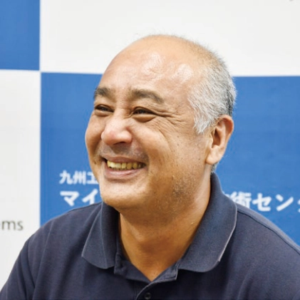
Professor Akiyoshi Baba
Center for Microelectronic Systems, Kyushu Institute of Technology
For this interview, we visited the Iizuka Campus of Kyushu Institute of Technology (Kyutech) to speak with Professor Akiyoshi Baba about operating and effectively utilizing the Center for Microelectronic Systems, one of Japan’s leading open semiconductor infrastructure platforms.
Brief History
2007–2019
Associate Professor, Center for Microelectronic Systems, Kyushu Institute of Technology
2019–2022
Professor, Organization for Promotion of Research and Open Innovation, Center for Microelectronic Systems, Kyushu Institute of Technology
2022–Present
Professor, Advanced Research and Social Cooperation Headquarters, Center for Microelectronic Systems, Kyushu Institute of Technology
2024–Present
Professor, Japan Special Zone for Semiconductor Human Resource Development and Innovation Promotion, Center for Microelectronic Systems, Kyushu Institute of Technology
Could you tell us about your current research?
I work on semiconductor microfabrication, particularly the integration technology of CMOS, MEMS, and fusion devices. Most recently, I have been studying semiconductor sensors capable of operating in extreme environments such as the deep sea.
At the same time, I have become deeply interested in the operation and effective use of core fabrication facilities, especially shared-use equipment, and I devote much of my time to this area.
From my early career, I worked extensively with microfabrication and analysis tools across many universities and research institutes. A common issue I observed was that once equipment broke down, it was often left unrepaired and essentially abandoned until the next grant could fund a replacement. I wanted to change this. For me, improving how facilities are managed and ensuring their effective use has become almost like a research theme of its own.
Of course, I still pursue research in science and engineering—fabrication of devices and sensors through microfabrication and process integration is one of my core strengths. But device development depends on connecting multiple pieces of equipment into a continuous process.
Without well-maintained and interconnected tools, you cannot complete fabrication and evaluation. Unfortunately, many labs still struggle with this. That is why I view research and facility operation as inseparable, and I focus on optimizing both for maximum impact.
How did you come to focus on this theme?
Since graduate school, I have been engaged in microfabrication, and I quickly realized that device fabrication can never be completed with a single piece of equipment. I often had to borrow tools from colleagues’ labs, visiting cleanrooms around the country. What struck me was how often I saw the same tool duplicated multiple times in one facility, while the essential idea of connecting tools into a complete process line was missing.
Devices require a continuous sequence of processes. If tools are not linked as a line, projects stall at the stage of elemental technology rather than reaching device completion. I repeatedly encountered this problem.
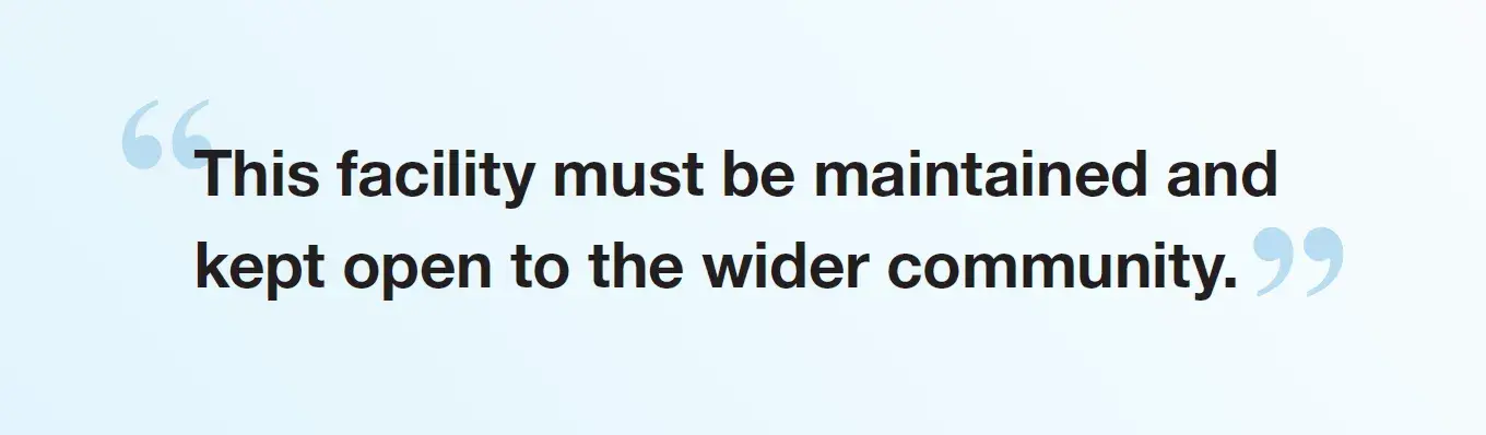
When I joined Kyutech in 1998, I was surprised to find a fully integrated 4-inch CMOS line already in place. I thought, “This facility must be maintained and kept open to the wider community.” That was exactly what had been missing elsewhere.
In 2018, when Professor Nakamura became director, the policy of opening the center was clearly emphasized. My own views aligned perfectly with the Center’s direction, and since then we have expanded initiatives focusing on openness and optimized operation.
Could you provide an overview of the Center for Microelectronic Systems?
The Center houses a fully integrated 4-inch wafer line capable of producing both CMOS and MEMS devices, covering everything from design to final evaluation. We welcome users from both academia and industry, with technical support provided by our staff.
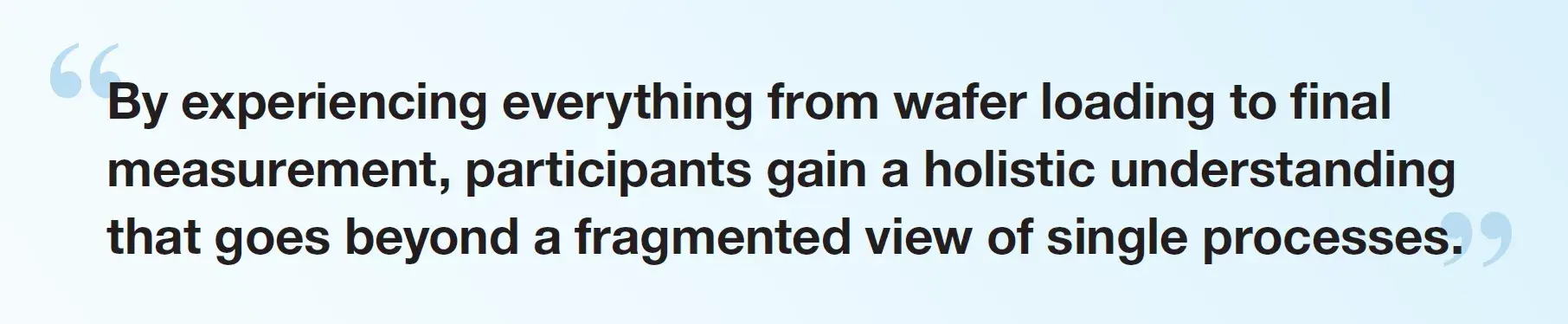
In education, we emphasize reskilling for professionals. Each year we run about 20 hands-on training sessions where participants fabricate and measure CMOS transistors through the entire process flow. By experiencing everything from wafer loading to final measurement, participants gain a holistic understanding that goes beyond a fragmented view of single processes.
Schedules are announced publicly, but we also arrange exclusive sessions upon request from companies. Another distinctive feature is that we do not assign staff to individual tools. Instead, all staff members are trained to handle the full CMOS and MEMS process chain, ensuring seamless training and support without handovers. This system began out of necessity when staff numbers were small, but it has proven highly effective and convenient for users.
What is the current status of the Center’s operation, and what are your future goals?
We have established an operating model that does not depend on university funding. Instead, we cover running costs through our own revenue streams. In terms of CMOS facilities and operation, we are among the top in Japan, pioneering the combination of education and equipment use.
By launching design training, opening equipment to external users, and hiring staff with self generated funds, we have realized true independence and openness. Looking ahead, I hope to see similar facilities established across the country. If such centers existed in multiple regions, users would no longer need to travel long distances, and research and development could proceed more efficiently.
The main challenges are recognition and location. We are situated in Iizuka City, about an hour’s drive from Fukuoka, in a mountainous area. Many visitors say they never expected to find a cleanroom here. Raising awareness to the point where people feel comfortable simply sending us an inquiry is one of our short-term goals. While our role in professional education is fairly well known, our function as an R&D facility is still not sufficiently recognized.
How does your Center differ from other institutions, particularly in handling user information?
We maintain an open-access policy for the facility, while handling all user information with complete confidentiality. Users are not obligated to submit reports, and it is up to them whether to acknowledge the Center in papers or presentations (we sometimes request it, but it is not mandatory). Restrictions on bringing in or removing materials are also relatively flexible.
Another unique feature is our independence from direct university funding, which gives us greater freedom and enables quick decision making to resolve issues efficiently.
How do you manage the risks associated with equipment downtime in a process line?
Because our facility is run as an integrated line, the stoppage of even a single tool can halt the entire process. This is especially detrimental when there are many external users, as the impact quickly cascades. To minimize downtime, we focus on preventive maintenance and close monitoring of equipment.
We are grateful for the rapid troubleshooting and flexible support from manufacturers, which helps us overcome even long lead times for parts. Ultimately, stable operation is the most critical factor in running a process line.
You’ve been using several Samco systems at your Center. Could you share your experience?
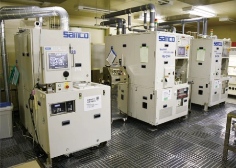
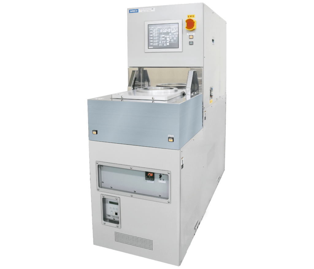
From left: First unit of Bosch process-compatible silicon deep etching system “RIE-800iPB”, Chlorine gas-based ICP etching system “RIE-101iPH”, and Fluorine gas-based ICP etching system “RIE-101iPH”
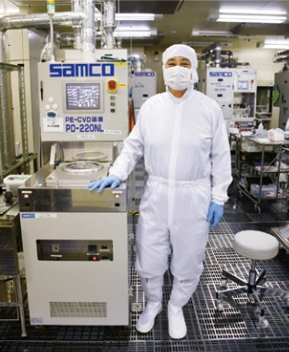
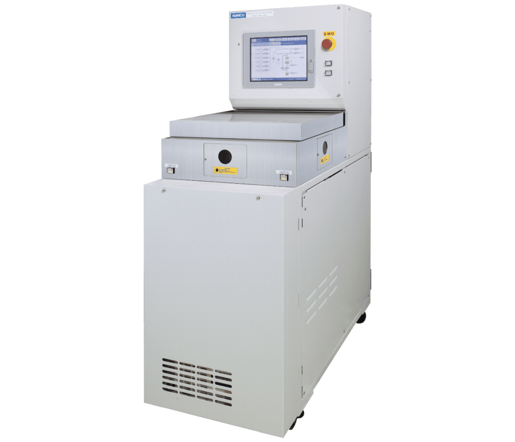
Professor Baba with Samco plasma CVD system “PD-220NL”
One of our most heavily used tools is Samco’s plasma CVD system, the PD-220NL. We use it for three types of films—amorphous silicon, silicon nitride, and silicon oxide—based on Samco’s standard recipes. Demand for these three film types is so high that reservations are almost always fully booked. To be honest, we could use a second system, but budget and space constraints make that difficult.
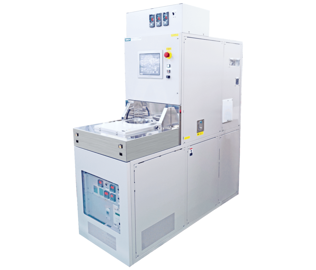
Our Bosch-process-compatible deep silicon etcher, the RIE-800iPB, has been running for more than a decade and still maintains highly stable performance with minimal variation, thanks to proper maintenance. In total, we operate five Samco systems, including two ICP etchers and the thick-film CVD tool PD-100ST, all of which continue to run stably over the long term.
What is most important in your day-to-day facility management?
Observation. Whether dealing with people or machines, the first step is careful observation. We look at whether the system is running efficiently and identify what is hindering it. Problems are rarely caused by individuals—they are usually structural. From there, we organize information, form hypotheses, and test them, just as in a scientific experiment.
Currently, the Center has 14 staff members, with about 10 directly involved in prototyping, training, and operations. Managing the balance between training sessions and machine time for users, while keeping the line running smoothly, is our top priority. When issues arise, we act quickly to correct them and continue improving step by step.
What are the specific benefits of your training programs for professionals?
Our through-process training gives participants the unique opportunity to experience the full device fabrication flow themselves. While single-process training is common, few programs allow participants to complete an entire CMOS device on a 4-inch line.
By building a tangible CMOS transistor, participants learn how each step connects, how processes depend on one another, and how line stoppages or cleanroom conditions affect outcomes. These are insights essential for real-world R&D.
How do you like to spend your free time?
I spend my weekends farming, playing tennis, or resting. I grow vegetables in my family’s fields and make the round trip on the expressway each week. Planning around the weather is always a challenge, but I enjoy how it resists human control— just like harvesting itself.
I also try to play tennis once a week, ideally three times, though weekday evenings are often too busy. After exercise, I make sure to rest well. I would love to nap with my cats, but it rarely works out that way.
Do you have any final thoughts?
Our goal is not simply to acquire high-performance equipment, but to use it to accelerate device development that leads to real-world applications. For this, an integrated line and a smooth operational framework are indispensable.
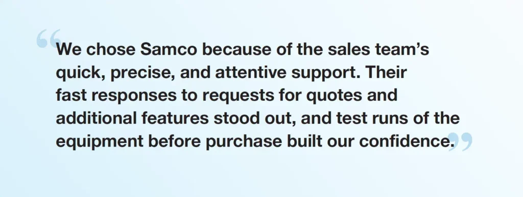
We chose Samco because of the sales team’s quick, precise, and attentive support. Their fast responses to requests for quotes and additional features stood out, and test runs of the equipment before purchase built our confidence. For long-term facility operation, both equipment performance and after-sales support are critical. Since installation, Samco systems have continued to run stably, which we value highly.
We look forward to Samco’s continued development of reliable, easy-to-use systems and long-term support we can depend on.
Thank you for taking the time out of your busy schedule to speak with us.