Dr. Satoshi Iwamoto
Professor, Research Center for Advanced Science and Technology, The University of Tokyo
In this interview, we visit the University of Tokyo’s Research Center for Advanced Science and Technology to talk with Dr. Satoshi Iwamoto about his research on topological photonics and other topics.
Brief History
Mar. 2002
Completed Doctoral program in Applied Physics, Graduate School of Engineering,
The University of Tokyo (Doctor of Engineering)
Sep. 2002
Research Associate, Institute of Industrial Science, The University of Tokyo
Jul. 2003
Lecturer, Institute of Industrial Science, The University of Tokyo
Sep. 2003
Lecturer, Research Center for Advanced Science and Technology, The University of Tokyo
Oct. 2007
Associate Professor, Research Center for Advanced Science and Technology, The University of Tokyo
Apr. 2009
Associate Professor, Institute of Industrial Science, The University of Tokyo
Apr. 2019
Professor, Institute of Industrial Science, The University of Tokyo
May 2019
Professor, Research Center for Advanced Science and Technology, The University of Tokyo
Awards
2000
Presentation Encouragement Award, Japan Society of Applied Physics
2005
International Conference on Solid State Devices and Materials Best Paper Award
2008
Activity Merit Award, Electronics Society, The Institute of Electronics, Information and Communication Engineers (awarded in 2008, 2012 and 2019)
2012
Young Scientist Award, Commendation for Science and Technology by the Minister of Education, Culture, Sports, Science and Technology
2017
APEX/JJAP Editorial Contribution Award (awarded in 2017 and 2020)
2018
The 23rd Microoptics Conference, Best Paper Award (awarded in 2018 and 2019 (24th))
2020
The 44th Laser Society of Japan / Distinguished Paper Award (Review Paper Section) (awarded in 2020 and 2021 (45th))
Selected as OSA Fellow (currently OPTICA Fellow) in 2021
2022
DOCOMO Mobile Science Award for Excellence in Basic Science
Please introduce your current research.
Our laboratory is working on photonic nanostructures, which are microstructures, mainly photonic crystals, for the control of light. Currently, we are focusing on three themes. First, topological photonics, second, diamond nanophotonics, and third, quantum nanophotonics. Topological photonics is an attempt to explore new functions and applications by rethinking the control and propagation of light based on a new concept of topology.
The behavior of electromagnetic waves, including light, is described by Maxwell’s equations, and photonics technology, which is widely used in communications and optoelectronics, has developed on this basis. However, there are still some issues to be solved in optical waveguides, which are necessary for small integrated optical circuits like electronic circuits. For example, structural defects and losses occur when optical waveguides are bent abruptly. In topological photonics, which is our focus, the concept of topology can be used so that even if there is a defect on the optical waveguide, light can travel through it without detecting the flaw. It may also be possible to realize the function of an optical isolator, like a diode, in which light travels in only one direction, with a small device. Realizing a waveguide in which light travels in only one direction is a very challenging research goal we are aiming for.
Diamond nanophotonics is the study of controlling light by fabricating photonic structures using diamonds instead of materials such as Si or compound semiconductors. This is part of the “Development of Quantum Interfaces for Construction of Quantum Computational Networks,” which is Goal 6 of the Moonshot R&D Program led by the Cabinet Office and for which Professor Hideo Kosaka of Yokohama National University is the project manager. Although diamond nanophotonics research is flourishing overseas, it is not very advanced in Japan. Our presentation at the upcoming conference will probably be the first paper on diamond nanophotonics in Japan. We are finally getting to the point where we can fabricate hollow structures such as air bridges.
Finally, we are working on quantum nanophotonics. This is related to the diamond nanophotonics I mentioned earlier, but it involves research related to the development of basic technologies for quantum interfaces. For example, in the Kosaka project, we are working on the concept of converting superconducting qubits into light in order to connect a quantum computer to another quantum computer.
Our mission is to develop quantum nanophotonics and to develop devices that serve as interfaces using photonic crystal nanocavities and other devices. This may be a dream-like technology that we are looking forward to seeing its future developments.
Please tell us more about topological photonics.
Topology is a branch of mathematics that studies and understands the shape of “things” in the big picture. A ball and a doughnut are well-known examples. Even if a ball is continuously deformed, it cannot be deformed into a doughnut without a “discontinuous” operation such as drilling a hole. In this case, the ball and the doughnut are topologically different.
In the field of condensed matter physics, new materials such as quantum spin Hall insulators and topological insulators have been discovered based on the topological understanding of the quantum Hall effect. In these materials, electrons flow in one direction at the boundary (edge) where two topologically different structures meet. This is called the topological edge state.
In 2008, British physicist Duncan Holden and his co-authors first showed that this topological edge state can occur in light propagating through periodic structures in the same way as electrons in crystals. Shortly after, in 2009, MIT demonstrated topological edge states in an experiment using microwaves. Microwaves have a lower frequency, and there are several materials that tend to change their response to electromagnetic waves when a magnetic field is applied. Therefore, it is easier to achieve topological edge states than with light. However, the realization of the topological edge state with light, which transmits electromagnetic waves in only one direction, as I mentioned at the beginning of this article, is still a way off. If we can achieve this, we will be able to create a compact optical isolator that physically travels in only one direction even if it has defects, which will pave the way for more sophisticated optical waveguides and the miniaturization and integration of related devices. This research has a very ambitious theme.
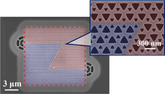
However, since research cannot proceed in a single step, topological photonics, which is widely studied around the world, is based on structures that can be fabricated using only semiconductors. One such structure is the Valley photonic crystal waveguide. Valley photonic crystals have time-reversal symmetry, so that some light travels to the right and some to the left at the same interface. In a valley photonic crystal waveguide with Z-shaped steep bends (Figure 1), inter-valley scattering is suppressed even at the bends, and good propagation characteristics are obtained.
Please explain how you started your research and how it has been progressing.
I originally planned to become an architect. My parents were in the construction business, and having watched them since I was a child, I somehow thought that I would be the one to take over the business. However, I decided to pursue a career in physics because of a physics class given by Mr. Hiroshi Kawakatsu when I was a sophomore in high school. He had published a book titled “Mr. Kawakatsu’s Physics Class”. In his classes, he would start with an experimental subject and have the students predict the results of the experiment from a list of options. Then he would conduct the experiment, and when the results were obtained, he would later explain why they were the way they were. It was that kind of class.
When I entered university, the themes of optical computers and optical information processing were gaining momentum, and I joined a laboratory in the field of optics, which led me to my current research. During my doctoral work, I studied nonlinear optics of semiconductors in the Kuroda-Shimura Laboratory. At that time, I was allowed to use the equipment in Arakawa Laboratory to fabricate samples.
I am very glad that I had the experience of designing, fabricating, evaluating, and analyzing the devices by myself. After graduation, I was fortunate enough to be accepted as a research assistant in Arakawa Laboratory, where I began my research on photonic crystals in earnest. I had been interested in topological photonics since it was published in a paper in 2008. In the meantime, Dr. Shun Takahashi of Kyoto Institute of Technology was working on a spiral three-dimensional photonic crystal called a chiral photonic crystal when he was still a student in Arakawa and Iwamoto’s lab. Dr. Takahashi came to discuss the topic at a conference in 2016 after hearing a presentation by a student in Prof. Hatsugai’s lab at Tsukuba University, who is very famous for topological physics, about the appearance of topological edge states in a similar photonic chiral structure. That was the beginning of our joint research. At about the same time, I was also doing research on the use of topological effects on elastic waves in the field of phononic crystals, which deals with sound waves. Prof. Hatsugai and I continue to collaborate on research, along with my ongoing discussions with a professor specializing in phononic crystals. These encounters accumulated and led me to start research on topological photonics.
If photonics and materials science are on the vertical axis, topology is like the horizontal axis. When we look at photonics from the horizontal axis of topology, there are concepts that are common to other fields. For this reason, since we started our research on topological photonics, we have expanded our interdisciplinary collaborations and collaborations with physics professors. We are trying to advance photonics with the concept of topology, and new phenomena realized in photonics may create new applications in different fields. I feel that this is another interesting aspect of conducting research in topology.
You have experience using Samco equipment, what are your impressions?
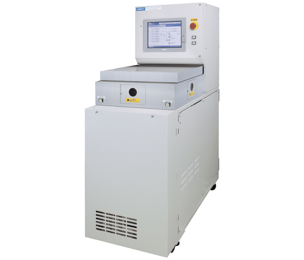
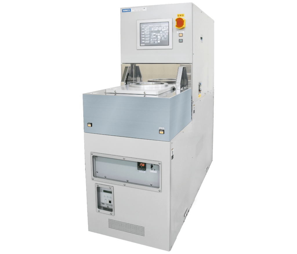
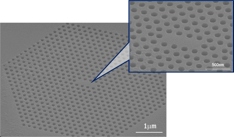
Samco’s equipment has been used by us for more than 20 years, from the ICP etching system RIE-101iP introduced in 1999 to the plasma enhanced CVD system to be delivered in 2023. The RIE-400iP, purchased in 2021, has a lower electrode that can be heated to 200°C and is used for diamond photonic crystals (Figure 2) and InP photonic crystals in the topological photonics process. The RIE-400iP has a more sophisticated control system and is easier to understand in many aspects.
In addition, I am satisfied with the support offered by Samco. They have been maintaining and taking care of the RIE-101iP that I have been using since the days of Prof. Arakawa, and I think they are quick to respond when it breaks down. I also like the fact that I can consult with them immediately about technical issues. In total, I feel that it is a great thing for us researchers to have such a manufacturer.
What you keep in mind in your daily research?
One is “Curiosity Driven,” and our laboratory places importance on thinking about what we find interesting. Of course, there are some research projects that have a specific target and are directed toward that target, but we believe that just going along the rails would not be interesting for the students. I also encourage students not to do research based on what I or someone else tells them to do, but to make up their own stories and plans and try to work on them, even if they fail. It’s not that they should just go ahead in the dark, but rather that they should give it a try if they are holding back. It’s a difficult balance.
Another thing I value is the connection among people. I try to visit students’ rooms as much as possible and have dinner with them so that we can discuss various topics and enjoy thinking. I think it is the best thing for students to spread their wings after working in Iwamoto Lab, so although I am not a behind-the-scenes supporter, I hope I can help them grow and give them a little boost.
Finally, I would like to talk with students not in a faculty-student relationship, but in a researcher-researcher relationship. Of course, if they ask me questions, I will teach them, but I don’t want them to think that what I say is absolute. There are new findings in what students say as well, and I value that. Furthermore, I tell those who are earning a doctorate, that one only truly earns their doctorate when they have as least a deep understanding of their subject as I do. After all, I am an expert.
Do you have a motto?
I am fond of the saying “every moment counts” which means that even a small amount of time should not be wasted. I do not use this phrase on a regular basis, so I may not call it my motto, but the purpose is right. Time is important, and I try to spend every moment carefully. Rest is also an important use of time, and I try to keep a clear distinction between on and off so that I don’t just do research all the time.
How do you spend your holidays?
I am very busy these days, so I don’t get long weekends off, but I like walking, and I walk several kilometers on the weekends.
I also like saunas. Sometimes I go to the sauna on a day when I am completely off, not even looking at my e-mail most of the time. Walking and saunas are good refreshments for me, because I can forget about my work.
Finally, do you have anything you would you like to say to Samco?
I would like to begin by saying how grateful we are to the company for supporting our research. I feel that Samco is supporting Japan’s cutting-edge research with their advanced technological capabilities. In recent years, I feel that in many places in Japan, there has been an increasing choice not to have fundamental or basic technology. While foundry services and the like are a good thing in some respects, on the other hand, I fear that locally cultivated technologies may be lost. I hope that Samco, as an equipment manufacturer that produces fundamental technologies, will continue to provide the latest process technologies. If I may say more, I would like to see Samco operate that technology in the form of an open laboratory, a platform that can be used by any researcher.
Thank you very much for taking time out of your busy schedule to speak with us.