Professor Reiji Hattori
Professor, Interdisciplinary Graduate School of Engineering Sciences, Kyushu University
Director, Center for Semiconductor and Device Ecosystem Research and Education (CSeDE), Kyushu University
For this interview, we visited Professor Reiji Hattori at the Center for Semiconductor and Device Ecosystem Research and Education (CSeDE) on Kyushu University’s Chikushi Campus to learn about his research in display electronics.

Academic Background
Apr. 1982 – Mar. 1986
School of Engineering, Osaka University (Department of Electrical Engineering)
Apr. 1986 – Mar. 1988
Graduate School of Engineering, Osaka University (Major: Electrical Engineering)
Apr. 1988 – Aug. 1989
Graduate School of Engineering, Osaka University (Major: Electrical Engineering)
Career History
Sep. 1989 – Mar. 1997
Research Associate, Faculty of Engineering, Osaka University
Apr. 1997 – Mar. 2009
Associate Professor, Graduate School of Information Science and Electrical Engineering, Kyushu University
Apr. 2009 – Present
Professor, Interdisciplinary Graduate School of Engineering Sciences, Kyushu University
Please tell us about your current research.
My research has focused on display electronics. This includes a variety of technologies such as AR/VR/MR1 displays, micro-LED displays, FPD backplanes, and touch panel systems. We’re also exploring eye-tracking technology.
Beyond that, we’re pursuing healthcare applications involving capacitive electrocardiography, which stemmed from our work on touch panels, as well as capacitive coupling-based wireless power transfer technology. While these topics may seem diverse, they are all closely connected to display technologies.
If I were to highlight one area, it would be our research on retinal scanning displays2 using holographic optical elements (HOEs), with the goal of future applications in smart glasses. This involves creating HOEs on eyeglass lenses and projecting laser light directly onto the retina.
This line of research started in response to a student’s interest in AR, and through extensive discussion, experimentation, and simulation, we arrived at our current approach. The technology holds the promise of enabling AR glasses that are significantly smaller and lighter than conventional displays.
While there are still many challenges to overcome—such as HOE design and fabrication, and laser control—we are tackling them step by step as we continue to advance the research.
1. AR (Augmented Reality) is a technology that overlays virtual information onto the real world. A common example is the display of CG images or text through the camera of a smartphone or tablet. VR (Virtual Reality) is a technology that lets you enter a virtual space by wearing dedicated VR goggles. MR (Mixed Reality) is a technology that merges the real and virtual worlds, allowing you to manipulate virtual objects as if they existed in the real world. It can be seen as a concept between AR and VR.
2. Retinal Scanning Display (RSD) is a display technology that directly projects images onto the retina. It is characterized by its ability to deliver high-quality, high-contrast visuals in a small and lightweight device, independent of the user’s vision.
Please tell us how you got started with your research and how it has evolved to the present.
During my doctoral studies, I researched the physical properties of amorphous silicon—a material that was attracting significant attention at the time for its potential in solar cells. Both academia and industry were deeply involved in studying it. My focus was on the Staebler–Wronski effect, a phenomenon where the electrical conductivity of amorphous silicon decreases when exposed to light.
After becoming a research associate, I wanted to pursue more development-oriented work and shifted my focus to thin-film transistors. Not long after, I had the opportunity to study at the University of Michigan in Professor Jerzy Kanicki’s lab, where I researched pixel circuits for OLED displays. That was the start of my work in display technologies.
A few years after returning to Japan, I was appointed as a visiting faculty member at the University of Tokyo’s VLSI Design and Education Center (VDEC), where I also worked on LSI design, including display driver ICs.
Since 2009, I have served as a professor at Kyushu University, where I’ve focused on display and semiconductor technology development through numerous collaborative projects with industry partners.
Please tell us about the Center for Semiconductor and Device Ecosystem (CSeDE).
The Center for Semiconductor and Device Ecosystem (CSeDE) was established on June 1, 2024, and held its official opening ceremony on October 25, welcoming distinguished guests including the university president and the vice governor of Fukuoka Prefecture. We commonly refer to the center as “CSeDE” (pronounced “seed”).
We spent about a year advocating for the center’s establishment as a new hub for research and education supporting the revitalized Kyushu Silicon Island. With strong backing from the university, we were able to move forward, and I have been honored with the role of director.
Since my student days, I’ve been involved in semiconductor fabrication and have gained experience across the entire spectrum—from semiconductor physics to circuit design. I’ve also worked with advanced materials such as organic and oxide semiconductors, and I hope to integrate the promising outcomes of university-led materials research with silicon LSI technologies. There is often a wide gap between academic research on materials and industrial development. I hope this center can serve as a bridge to close that gap and strengthen collaboration between academia and industry.
Please share your outlook on the future of your research.
With the semiconductor boom currently underway in Kyushu, I would like to take on the challenge of exploring new semiconductor applications grounded in display technologies. Specifically, I see great potential in areas such as computer graphics processing and image recognition chips for AR/VR/MR head-mounted displays, as well as ICs for µ-LED displays.
We are currently working on hardware development for AR/VR/MR, and I believe these technologies will increasingly require high-speed video processing—making them a key application area for cutting-edge semiconductors. Likewise, µ-LED displays, which are considered a promising next-generation flat panel display (FPD) technology, also require dedicated driver and controller ICs.
In this way, I plan to continue research at the intersection of display and semiconductor technologies. Although Japan’s display industry is not currently thriving, the global market continues to expand steadily, with active technological innovation taking place worldwide. As signs of a semiconductor industry revival begin to appear in Japan, I hope my research can contribute to a similar revitalization in Japan’s display sector as well.
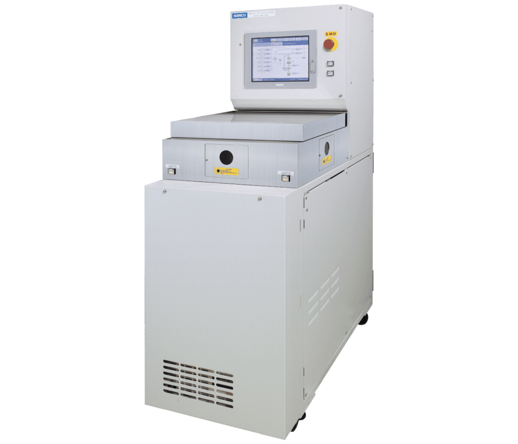
You currently use one of our systems. Could you share your thoughts on it?


We use the parallel plate RIE system RIE-10NR. Its compact footprint makes it easy to use without taking up too much space in our cleanroom. Although the system was purchased more than 20 years ago, it continues to operate without issues thanks to regular maintenance. It was also the first system in our lab where recipes could be input via a touchscreen interface, and processes could be started with the press of a button. This level of user-friendliness makes it particularly well suited for research applications and easy for students to handle.
Because we use the system for etching organic materials, some internal components of the reaction chamber were replaced with glass. Compared to metal, glass introduces fewer contaminants when processing organics, which is a key advantage.
Additionally, we greatly appreciate Samco’s flexibility in supporting us—for example, by implementing software that allows for stepwise discharge in areas where plasma is difficult to ignite. It is the most useful semiconductor process tool in our lab.
What do you keep in mind in your day-to-day research?
In my research, I make it a point to focus only on topics that genuinely interest me. If I don’t find something engaging, students probably won’t either. Conversely, I’m often inspired by the things that spark curiosity in my students.
In the lab, I strive to create an environment where students can take initiative in their research. I respect their interests and encourage open dialogue and idea-sharing. When deciding on research themes, I actively incorporate student input. If they find a topic compelling, they’re more likely to engage wholeheartedly with the work.
When we hit a roadblock, I work together with students to revisit discussions or review experimental data, searching for new possibilities. One of the advantages of doing research at a university is the freedom to choose your own topics—something that isn’t always possible in a corporate setting. In that sense, I feel very fortunate to be working in academia.
Please share a word or lesson you value.
I’ve always had a fondness for the character “励” (rei) used in my name. While it may not be a standard character for names, it appears in words like “encouragement” (shōrei) and “diligent practice” (reikō), both of which convey a strong sense of initiative and positivity. I feel that this single character carries the energy needed to lead a bright and optimistic life, and I’m grateful to my parents for giving it to me.
A research career is rarely smooth, but I try to overcome difficulties with a positive outlook, always keeping the spirit of “励” close to heart. I hope my students will also embrace this attitude as they pursue their own paths.
How do you usually spend your days off?
I don’t really have any hobbies of my own, so on my days off, I try to live frugally and spend as much time as I can with my wife. Since I’m usually not home very often, I make it a point to cherish time with my family. If I had to name something, I’d say I enjoy visiting shrines and ancient burial mounds in Kyushu. My family is from Nara, so I’ve always had an interest in ancient history.
Any final words?
I find Samco’s equipment compact, user-friendly, and ideally suited for university laboratories. While some believe that research should be conducted with mass-production-ready systems from the outset to ease the transition to full-scale manufacturing, I think otherwise.
To explore new ideas freely, dedicated R&D equipment is essential. Even in the corporate world, I believe having tools designed specifically for research and development is important, as mass-production equipment often comes with many limitations.
I hope Samco will continue to develop useful tools for universities and actively pursue equipment development that incorporates new technologies.
Thank you for taking the time out of your busy schedule to speak with us.