language
Samco Inc.
USA Website Next Gen
Application of Aqua Plasma® for Microbumps
You are here:
- Home
- News & Events
- Technical reports
- Application of Aqua Plasma® for…
Samco Inc.
As our information-driven society progresses, semiconductor packages are becoming more sophisticated, functional, and compact. Although semiconductor chips can be densely connected using flip chips with gold or solder bumps, micro bumps with Cu posts[1] are widely used to address rising gold prices, electrical characteristics requirements, and the increasing number of I/Os. As shown in Figure 1, microbumps are formed by sputtering, photolithography, and electrolytic plating. In-process plasma treatment is used to improve the wettability and adhesion of the plating solution. Oxygen plasma is primarily used, but it presents challenges: the plating solution cannot penetrate fine patterns, and seed Cu is excessively oxidized, leading to performance degradation. Typically, the oxidized Cu layer can be removed with dilute sulfuric acid, but in some cases, such as low-density films deposited for stress relaxation, the oxidation is too deep to remove.
The reduced-pressure steam plasma[2] (Aqua Plasma®) that we have developed[3] exhibits excellent hydrophilic effects, prevents Cu oxidation, and reduces oxidized Cu. In this report, we present the evaluation results of actually fabricated microbumps.
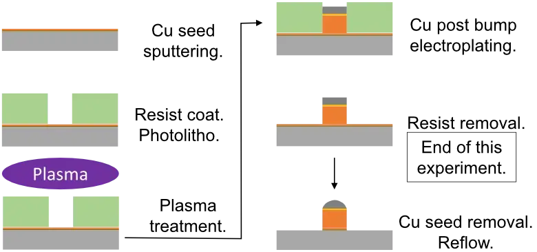
The sample was an φ8 inch Si wafer sputter-deposited with Ti (30 nm) and Cu (200 nm) for seeding. Thick film photoresist (Tokyo Ohka Kogyo, PMER🄬 P-BZ4000), widely used for microbump fabrication, was applied to the sample, modified by Aqua Plasma® (AQ-2000), and the contact angle of pure water was measured.
The sample was then treated with AQ-2000 for 5 minutes, and microbumps were formed by electrolytic plating of Cu, Ni, and SnAg at thicknesses of 35 µm, 2 µm, and 15 µm, respectively, followed by removal of the resist with a stripping solution (ST-120, Tokyo Ohka Kogyo Co., Ltd.). The resist and microbumps were observed by SEM (Scanning Electron Microscope).
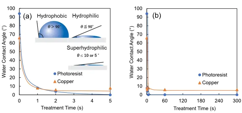
The contact angle measurement results are shown in Figure 2. The photoresist was initially hydrophobic with an initial value of 94°, but after 1 second of treatment it became super hydrophilic with a value of 8°, and further treatment from 5 to 300 seconds resulted in a contact angle of 1°. Seed Cu had an initial value of 66°, but was super hydrophilic to 8° after 1 to 300 seconds of treatment.
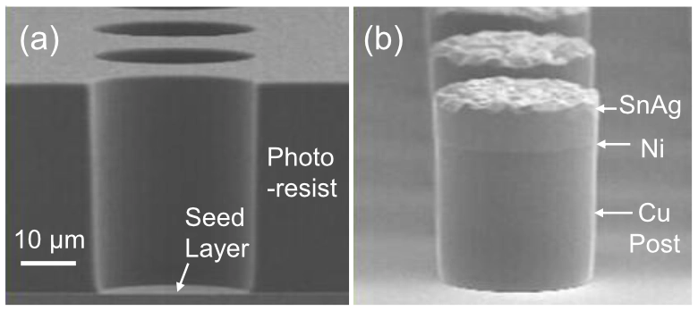
The results of SEM observations are shown in Figure 3. Figure 3a shows plasma treated resist before plating, and Figure 3b shows micro bumps after plating and resist stripping. No abnormalities such as oxidation discoloration or shape change of seed Cu were observed even after 5 minutes of treatment. There were no abnormalities such as deformation or surface roughness at the interface with seed Cu, and bumps were formed in a form opposite to the resist before plating.
These results show that Aqua Plasma® is useful for filling fine patterns with plating solution and avoiding Cu oxidation. However, descum was not confirmed in this study. Some of the resist was not stripped and remained. We aim to improve the process by optimizing conditions and expanding the process.
We would like to express our deep appreciation to Tokyo Ohka Kogyo Co.
K. Toriyama, K. Okamoto, S. Kohara, and Y. Orii, “Development Status of Micro-Bump Interconnection Technologies,” J. Japan Inst. Packag. vol. 14, no. 5, pp. 372-376, 2011.
Samco NOW Vol. 94, 96, 100, 102.
H. Terai, T. Hashimoto, H. Nakano, and O. Tsuji, “Reduction and Surface Treatment for Oxidized Copper Electrodes by Water Vapor Plasma,” IEEE CPMT Symposium Japan, pp. 11-14, 2019.