Introduction
As semiconductor devices continue to become more miniaturized and highly integrated, control of the etching process at the atomic level has become essential. Among various technologies, Atomic Layer Etching (ALE) is receiving significant attention.
ALE is a cyclic process composed of alternating modification and removal steps, each of which involves a self-limiting reaction.[1] [2] During the modification step, the etchant adsorbs to the surface of the substrate, reacts with a single atomic layer, and forms a modified layer. This reaction proceeds in a self-limiting manner and does not proceed further once the layer is fully modified.
In the removal step, only the modified layer is etched, while the substrate and unreacted atoms are not affected. Due to these two self-limiting reactions, the thickness of the atomic layer removed per cycle remains constant, yielding the following process advantages:
- High-Precision Depth Control
The etch amount per cycle is stable in the range of several angstroms, enabling highly precise control of etching depth.
- Low Damage
The use of low-energy ions minimizes damage to the substrate and reduces defect formation.
- High Uniformity
Uniform etch depth across the wafer is achieved, providing excellent process reproducibility.
Based on these features, ALE has been applied to the fabrication of advanced devices such as FinFETs, 3D NAND, power devices, and compound semiconductors.
ALE can be implemented using several modes, including Plasma ALE, Thermal ALE, and Plasma-Thermal ALE.[3] [4] Samco is engaged in extensive research and development related to each of these methods. This article introduces the features of Samco’s ALE systems, as well as related process data.
ALE Systems
Samco has developed ALE capabilities by incorporating ALE functions into conventional Inductively Coupled Plasma (ICP) etching systems. As a result, a single system can be used for both ICP etching and ALE. Samco’s ALE systems incorporate the following two technical capabilities:
- Precise Control in the Low Bias Power Range
Samco systems include an attenuator and switching unit in the high-frequency transmission line of the bias power supply. In order to ensure that only the modified layer is etched during ALE, precise control in the extremely low output range is required, and the optimal control range varies depending on the material. The attenuator adjusts the ion energy reaching the substrate from the plasma, enabling precise control in the low bias-power range. In addition to the attenuator, Samco also enhances control performance through bias power monitoring using a power meter, ensuring stable and repeatable operation.
- Improvement of Gas Switching Speed
To improve gas switching speed in the reaction chamber, an ALE specific gas box is positioned in close proximity to the chamber. Since ALE requires switching between gases for the modification and removal steps, minimizing the switching time is crucial for throughput improvement. Gas switching time depends strongly on both the length of the gas lines and the valve response time. Therefore, by shortening the piping configuration, switching speed is increased, modification reproducibility is maintained, and cycle time is reduced.
In addition, in Quasi-ALE (a process similar to ALE that does not involve self-limiting reactions) the etch depth per cycle is determined by the thickness of the deposited etchant during the modification (deposition) step. Compared to ALE, higher gas switching precision is required to ensure reproducibility.[5]
Process Data
A GaN/AlGaN chip sample was mounted with oil onto a 6-inch silicon wafer coated with Thermal SiO2 and polyimide tape, followed by ALE. Chlorine (Cl2) gas was used for the modification step, and argon (Ar) gas was used for the removal step.
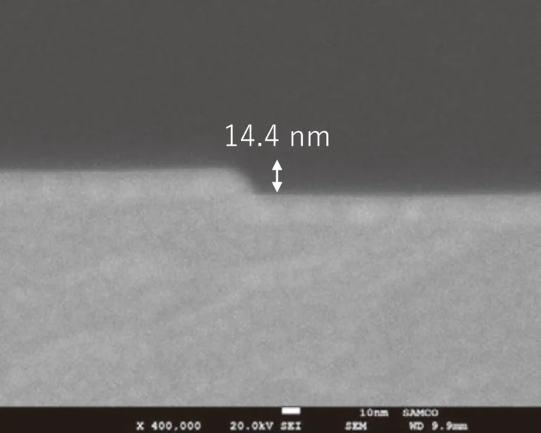
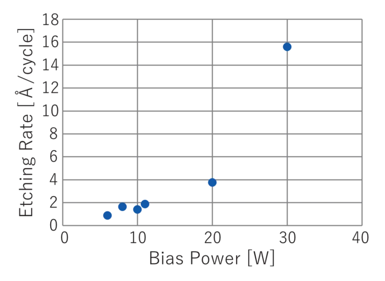
Figure 1 shows a scanning electron microscope (SEM) image of a trench structure with a width of 500 nm, processed by ALE and with the SiN mask removed. After 88 ALE cycles, the etch depth reached 14.4 nm. The etch rate was 1.63 Å/cycle, demonstrating true atomic-scale etching control.
Figure 2 shows the results of an etch rate measurement per cycle under varying bias power conditions. A stable etch rate was observed in the 6–11 W range, indicating that the self limiting nature of ALE was successfully maintained.
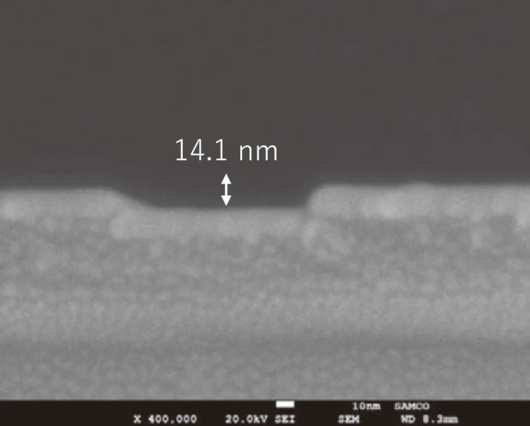
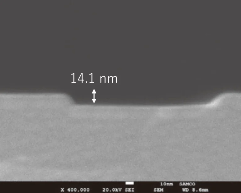
Figure 3. SEM images of GaN/AlGaN ALE-etched trenches with (a) 100 nm width and (b) 200 nm width.
Figure 3 shows SEM images of trenches with widths of 100 nm and 200 nm, processed under the same conditions as the 500 nm trench. In both cases, the etch depth was 14.1 nm, confirming suppression of the microloading effect and achievement of excellent depth uniformity, regardless of the pattern width.
Conclusion
This technical report has introduced the features of Samco’s ALE systems, which enable atomic-level etching control, and has presented representative process data. ALE demonstrates advantages in etch depth precision and damage suppression, areas where conventional ICP etching faces challenges.
Future reports will introduce further evaluations related to substrate damage and device performance characteristics.
Acknowledgements
We would like to express our sincere gratitude to Nagoya University for providing the samples used to obtain the SEM images featured in this technical report.
References
[1]Keren J. Kanarik, et al., “Overview of atomic layer etching in the semiconductor industry,” Journal of Vacuum Science & Technology A, 33, 020802 (2015)
[2]Satish D. Athavale, et al., “Realization of atomic layer etching of silicon,” J. Vac. Sci. Technol. B, 14(6), Nov/ Dec 1996
[3]Xia Sang et al., “Physical and chemical effects in directional Atomic Layer Etching,” Journal of Physics D: Applied Physics, 2020
[4]J. W. Daulton, et al., “Selectivity Control in AlGaN/ GaN Atomic Layer Etching,” AVS ALE Workshop, 2015
[5]Sonam D. Sherpa et al., “Quasi-atomic layer etching of silicon nitride,” Journal of Vacuum Science & Technology A, 35, 01A102 (2017)