On April 24, 2026, Samco participated in the OneNano Mid-Atlantic Chapter’s Spring Meredith Meeting, held at Princeton University’s Princeton Materials Institute.
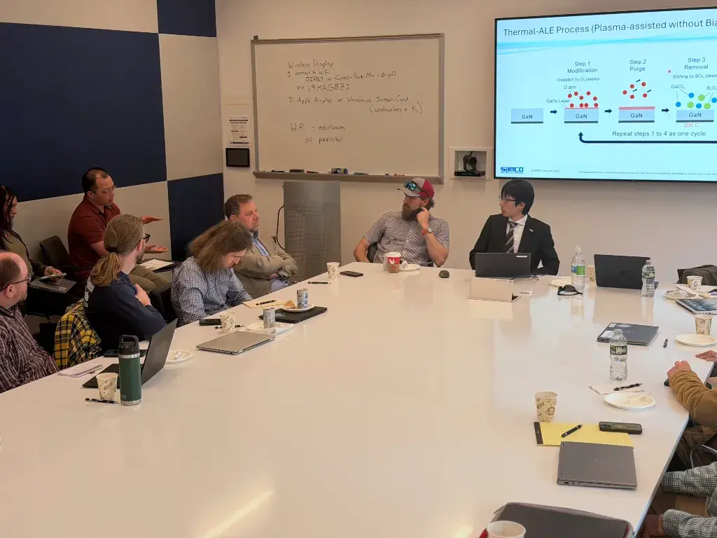
As a sponsor of the event, Samco delivered a technical presentation on Atomic Layer Etching (ALE) technologies for atomic- to nanoscale processing. The presentation introduced Samco’s expertise in both thermal ALE and plasma-enhanced ALE, with a particular focus on plasma-assisted ALE processes for advanced compound semiconductor device fabrication.
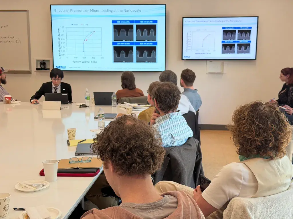
During the session, Samco discussed key factors in nanoscale etching, including process control, surface modification, material selectivity, and damage reduction. Process examples included applications for AlGaN/GaN HEMT fabrication and diamond etching, highlighting how ALE can support emerging device structures that require precise, low-damage material removal.
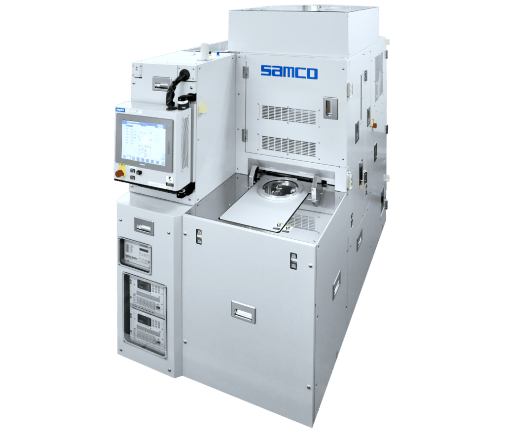
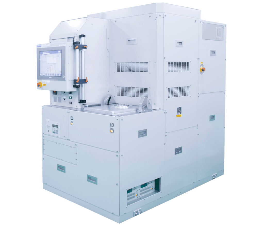
Samco also introduced how ALE capability can be integrated into its RIE-400iP and RIE-800iP ICP-RIE platforms. By combining conventional ICP-RIE processing and ALE functionality within a single system, these platforms allow researchers and device engineers to expand process flexibility while reducing the need for separate dedicated etching tools.
As device structures continue to scale and new materials are introduced into semiconductor and photonic applications, precise etching technologies are becoming increasingly important. Samco continues to develop ALE processes for novel materials and advanced device structures, while supporting customers through process development, equipment customization, and technical collaboration.
Samco appreciates the opportunity to engage with the OneNano Mid-Atlantic research community and looks forward to continuing discussions with researchers and engineers working in atomic- to nanoscale fabrication.
For more information about Samco’s ALE-capable ICP-RIE systems, please contact our sales team.
About Samco Inc.
Samco Inc. (TSE: 6387) stands for Semiconductor And Materials Company, is a leading manufacturer of processing equipment for the semiconductor and related industries. Founded in Kyoto, Japan in 1979 by Osamu Tsuji, Samco has nearly five decades of experience and has installed more than 5,000 systems worldwide. Its equipment and thin film technologies are widely adopted in the fabrication of semiconductor devices, including SiC/GaN power and RF devices, GaAs VCSELs, InP Laser Diodes, MEMS, BAW/SAW Filters, advanced packaging, and emerging quantum and photonic devices.
Learn more at https://www.samcointl.com/about/
Company Contacts:
TSUCHIHASHI, Atsushi
Public Relations
Phone: 81-75-621-7841
E-mail: tsuchihashi@samco.co.jp
DUNCAN, Megan
Public Relations
E-mail: megan.duncan@samco.co.jp