Compared to the mainstream semiconductor Si, the wide bandgap semiconductor 4H-SiC has excellent material qualities including higher electrical breakdown strength and higher thermal conductivity. Therefore, 4H-SiC has been studied in recent years as a new material to improve miniaturization and energy saving in power devices.
Currently, it is being developed not only for device fabrication but also for practical applications in the automotive and power supply industries. SiC MOSFETs (Metal Oxide Semiconductor Field Effect Transistors) are one example of commonly used 4H-SiC power devices that surpass Si power devices in terms of high voltage endurance, low on-resistance, and high-speed switching.
Trench type SiC MOSFETs are being developed and have shown that they are capable of achieving a reduced on-resistance, which is highly demanded in current devices. We have been developing a trench etching process using plasma dry etching and deposition of the gate insulator using ALD (Atomic Layer Deposition) and PECVD (Plasma Enhanced Chemical Vapor Deposition). These processes are required for manufacturing trench type SiC MOSFETs.
In this report, we will highlight the SiC trench etching and gate insulator deposition results.
In SiC trench etching, it is vital to achieve a high SiC etch rate and high etch selectivity (SiC/SiO2), while at the same time controlling the sidewall smoothness and etching shape (rounded trench corner and perpendicular sidewall). Four-inch and six-inch wafers are currently the mainstream substrates for 4H-SiC devices.
The ICP etching systems we developed are RIE-400iP/iPC for 4-inch wafers and RIE-800iP/iPC for 6-inch wafers. These ICP etching systems can obtain a SiC etching rate of 450 nm/min or more, etch selectivity of 5 or more and etching depth uniformity of ±3% or less. We have also been able to attain the desired etching feature shape (perpendicular sidewall with no micro-trench).
The SiC trench etching result using the RIE-800iP is shown in Fig. 1. There is a problem with the electric field tending to concentrate on the bottom corner of the trench in the gate insulator under high device bias. This induces an insulator breakdown at the trench bottom. Thus, the shape of the trench bottom is generally rounded by annealing at about 1500°C after etching.
We developed a new trench etching process that has rounded corners in the trench bottom without annealing. This etching result is shown in Fig. 2. We are now able to optimize the etching conditions and adjust the roundness of the trench bottom in accordance with a customer’s specified trench width and mask thickness.
Figure 1. SiC trench etch result using RIE-800iP
Etch depth : 1.98 μm, Etch rate : 464 nm/min, Etch selectivity : 5.5 (SiC/SiO2)
It is necessary for trench type SiC MOSFET gate insulators to have thin sidewalls for good current flow and thick trench bottoms to increase the breakdown voltage. A gate insulator for SiC power devices is generally formed by SiO2 which is deposited using a combination of ALD and PECVD. The breakdown voltage (BV) and hysteresis in capacitance-voltage (C-V) are higher and smaller, respectively, when SiO2 is deposited using ALD than if PECVD was used. However, SiO2 deposited using ALD is conformal in the trench. On the other hand, with SiO2 deposited using our Cathode-Coupled PECVD, it is possible to increase the thickness of the trench bottom. Moreover, the hysteresis in C-V measurement can be resolved by post deposition annealing.
We tried the deposition of gate insulators using an ALD and PECVD multi-layer, which consisted of SiO2 being deposited on a device using ALD and then depositing another layer on top using PECVD. We fabricated a trench type SiC MOSFET and measured the device characteristics in order to evaluate this gate insulator. We were able to obtain good BV and voltage drain source (Vds) results using this method. The results of SiO2 deposition in the trench are shown in Fig. 3.
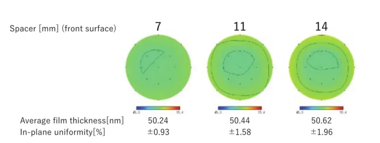
When the spacer height was varied to 7 mm, 11 mm, and 14 mm, no significant fluctuation was observed in the average film thickness. A slight increase in thickness near the wafer edge was noted; however, in-plane uniformity remained within ±2%, indicating excellent reproducibility.
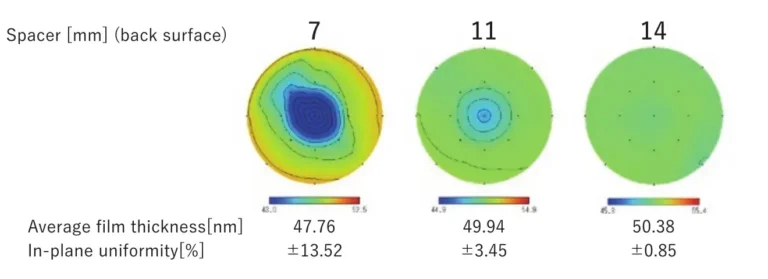
In contrast, the back surface results shown in Figure 3 exhibited clear improvements in both average thickness and in-plane uniformity with increasing spacer height.
A consistent pattern of central thinning and edge thickening was observed, suggesting limited plasma radical transport to the center of the wafer.
Figure 4 presents the ratio of back surface-to-front surface film thickness. As spacer height increased, the ratio approached unity, reaching 0.99 at 14 mm. This indicates nearly equivalent deposition on both surfaces.
Further analysis of the AlOx films deposited under the 14 mm condition showed refractive index values ranging from n = 1.705 to 1.712 on both surfaces. Wet etch rate (W.E.R.) testing with respect to buffered hydrofluoric acid (BHF) yielded rates of 87.6 nm/min on the front surface and 85.7 nm/min on the back surface, confirming the uniformity of film composition and structure.
These results collectively demonstrate that a spacer height of 14 mm enables highly uniform dual-surface deposition in both film thickness and material quality.
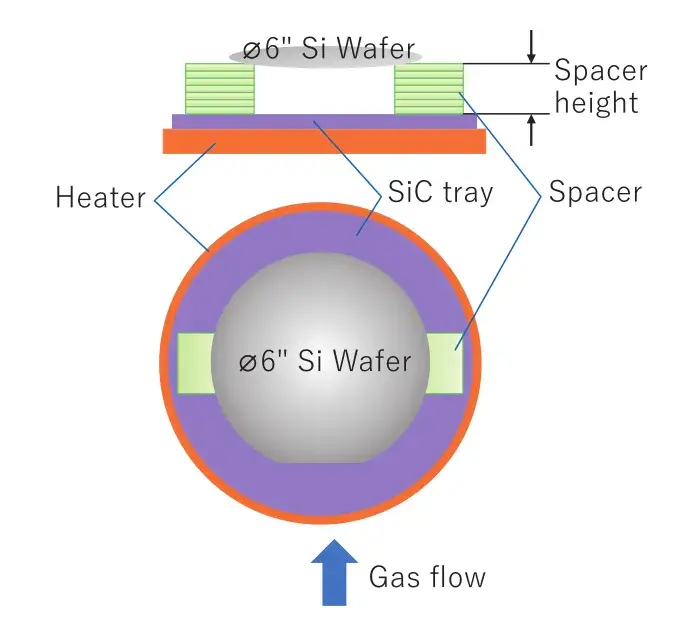
This study investigated a method for simultaneous dual-surface deposition of AlOx films on silicon wafers using the Plasma Enhanced Atomic Layer Deposition (PEALD) technique, in which wafers were suspended within the chamber using spacers. Spacer heights were varied between 7 mm and 14 mm. The results indicated that increasing the spacer height led to a reduction in thickness differences between the front surface and back surface. At a height of 14 mm, the film thickness ratio reached 0.99, demonstrating nearly equivalent deposition on both surfaces.
Furthermore, under the 14 mm condition, the refractive index and wet etch rate measurements revealed negligible differences between the front surface and back surface. These findings confirm that uniformity was achieved not only in film thickness but also in film quality.
Future work will focus on extending this approach to other film materials and deposition conditions, with the aim of further optimizing the process and broadening its applicability.