language
Samco Inc.
USA Website Next Gen
What is Atomic Layer Deposition (ALD)?
You are here:
- Home
- News & Events
- Tutorials
- What is Atomic Layer Deposition…
Atomic Layer Deposition (ALD) is a thin-film deposition technique that utilizes self-limiting surface chemical reactions to achieve precise layer-by-layer growth. By alternately introducing and exhausting two or more reactants into the reaction chamber, ALD enables excellent film thickness control, superior step coverage, and high conformality. As demand for high-performance semiconductor devices, MEMS, and optical coatings increases, ALD is gaining attention for its ability to deposit high-quality films with atomic-scale precision.

ALD offers several advantages over traditional deposition methods such as Plasma Enhanced Chemical Vapor Deposition (PECVD) and Physical Vapor Deposition (PVD)/sputtering:
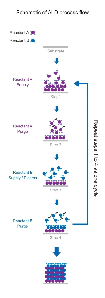
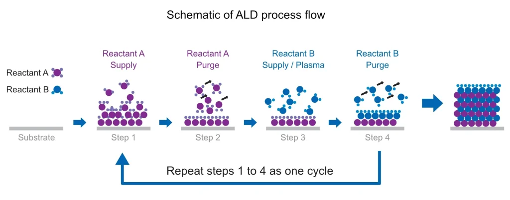
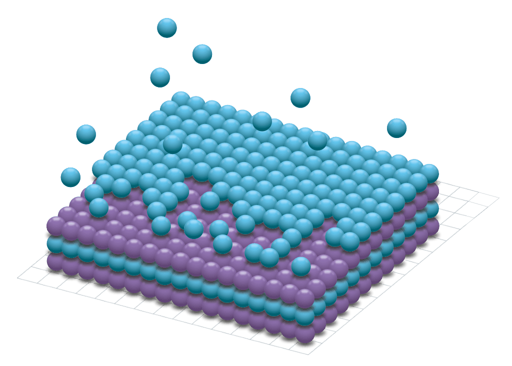
ALD operates based on a self-limiting, cyclic process that deposits atomic layers onto a substrate. A standard ALD cycle consists of four steps:
Step 1: Reactant A adsorption – The precursor molecules are introduced into the chamber and chemically adsorbed onto the substrate surface.
Step 2: Purge – Excess precursor and by-products are removed from the chamber.
Step 3: Reactant B exposure – An oxidant or nitriding agent reacts with the adsorbed layer, forming the desired film.
Step 4: Purge – Excess reactants and by-products are purged from the chamber.
Each ALD cycle consists of Steps 1 to 4. Through repetition of this cycle, atomic layers are deposited onto the substrate one by one with precision.
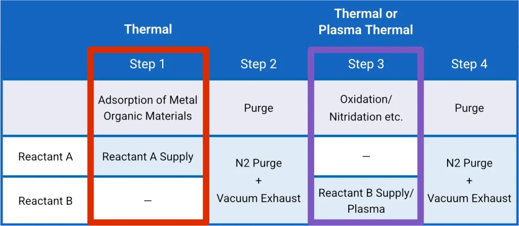
There are two types of ALD methods: thermal ALD and plasma enhanced ALD. The difference between the two types is whether the oxidation or nitridation in Step 3 is done by thermal alone or by a combination of thermal and plasma. Plasma is not used for chemical adsorption of Metal organic materials in Step 1. In this step, only heat is used.
Heil, S. B. S., et al. “Deposition of TiN and HfO2 in a commercial 200mm remote plasma atomic layer deposition reactor.” Journal of Vacuum Science & Technology A 25.5 (2007): 1357-1366.
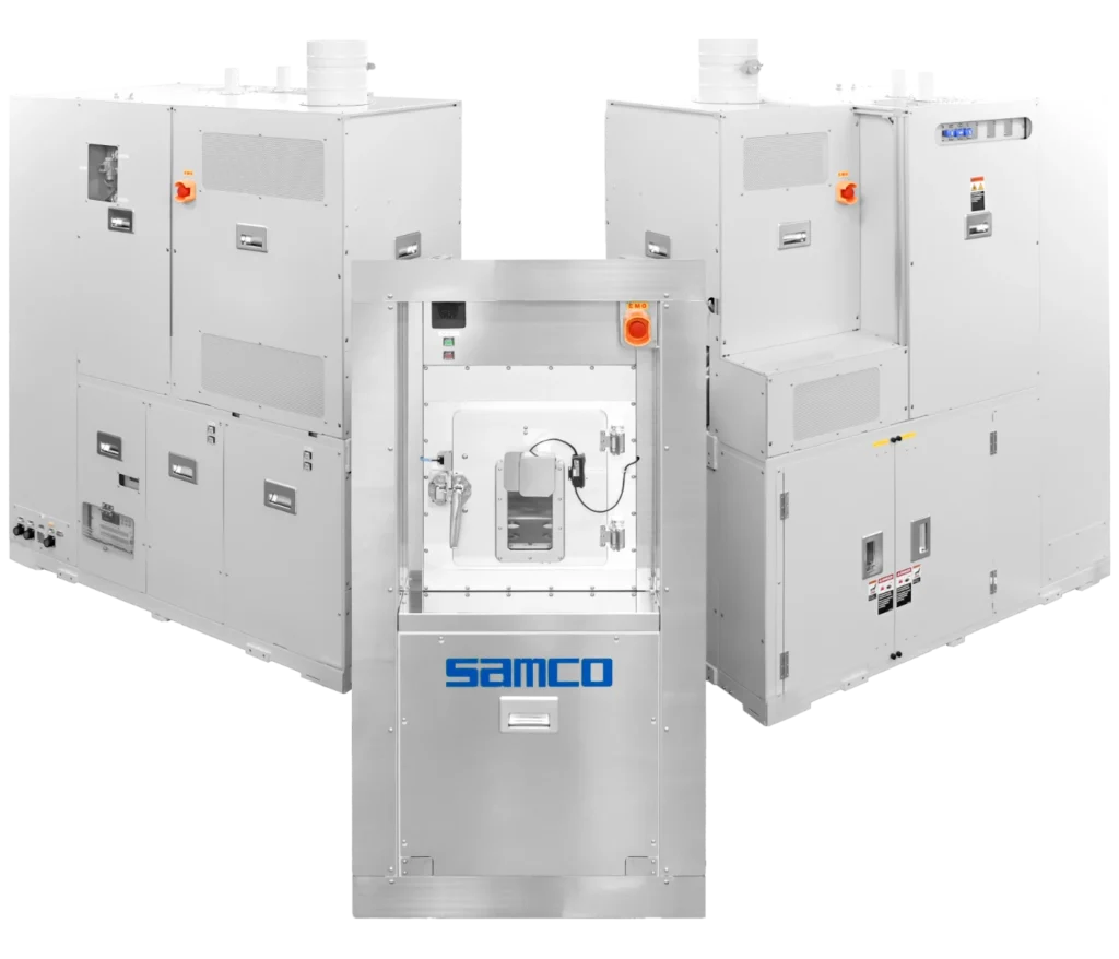
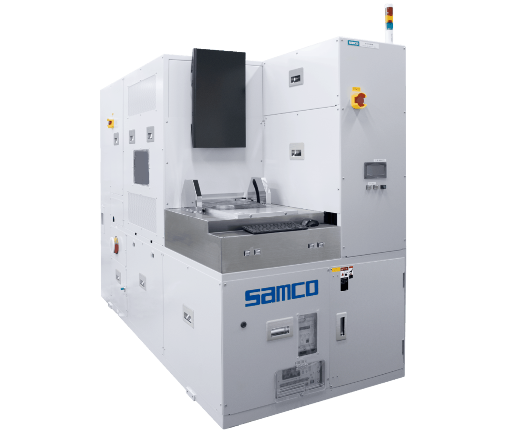
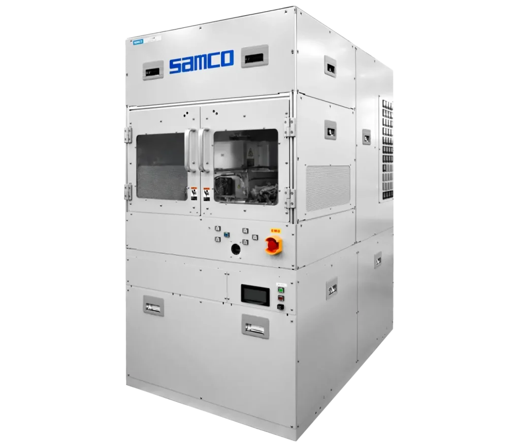
Samco’s atomic layer deposition (ALD) systems enable precise, uniform thin-film coatings with excellent step coverage, even on high-aspect-ratio structures. These capabilities are essential for applications requiring high-performance insulating, passivation, and barrier layers. Below are examples of ALD process applications: