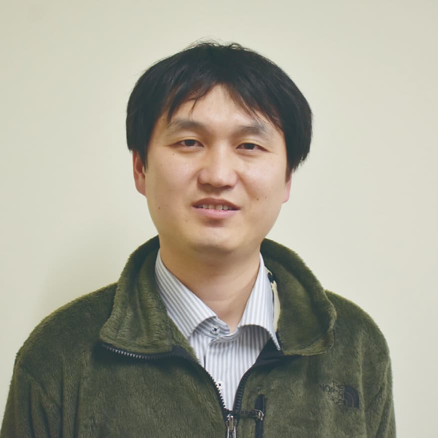
Matthew – Supporting customers across the U.S.
Meet Matthew Alexander, Program Manager at Samco’s U.S. branch, and learn about his career journey, team culture, and work supporting semiconductor R&D.
Meet Matthew Alexander, Program Manager at Samco’s U.S. branch, and learn about his career journey, team culture, and work supporting semiconductor R&D.
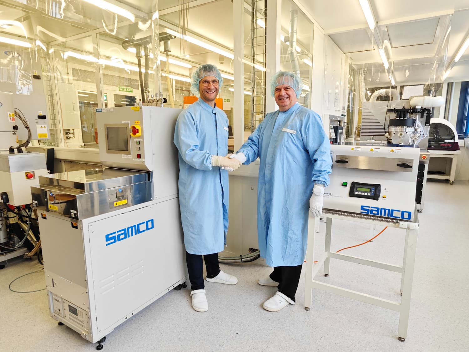
DTU Nanolab, Denmark’s national nanofabrication facility, will expand its silicon DRIE infrastructure with Samco’s cassette-loading RIE-800iPBC system to support advanced MEMS, photonics, and microfabrication research.
Professor Mikihiko Oogane discusses TMR sensors, quantum spintronics, and brain–information interfaces in magnetic sensing research at Tohoku University.
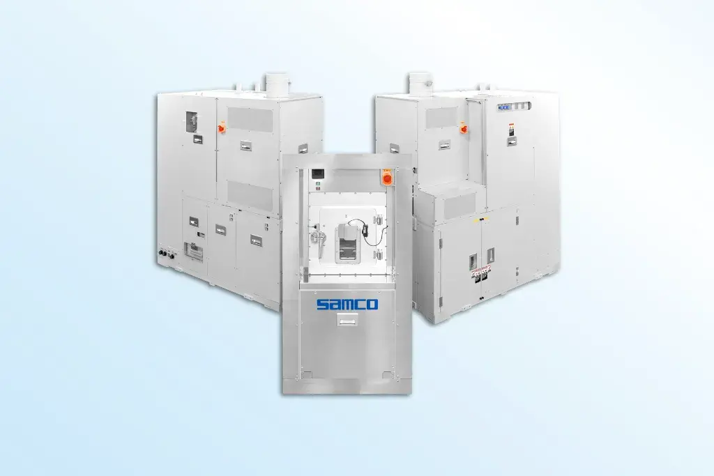
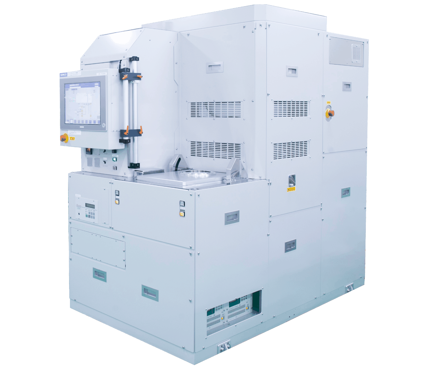
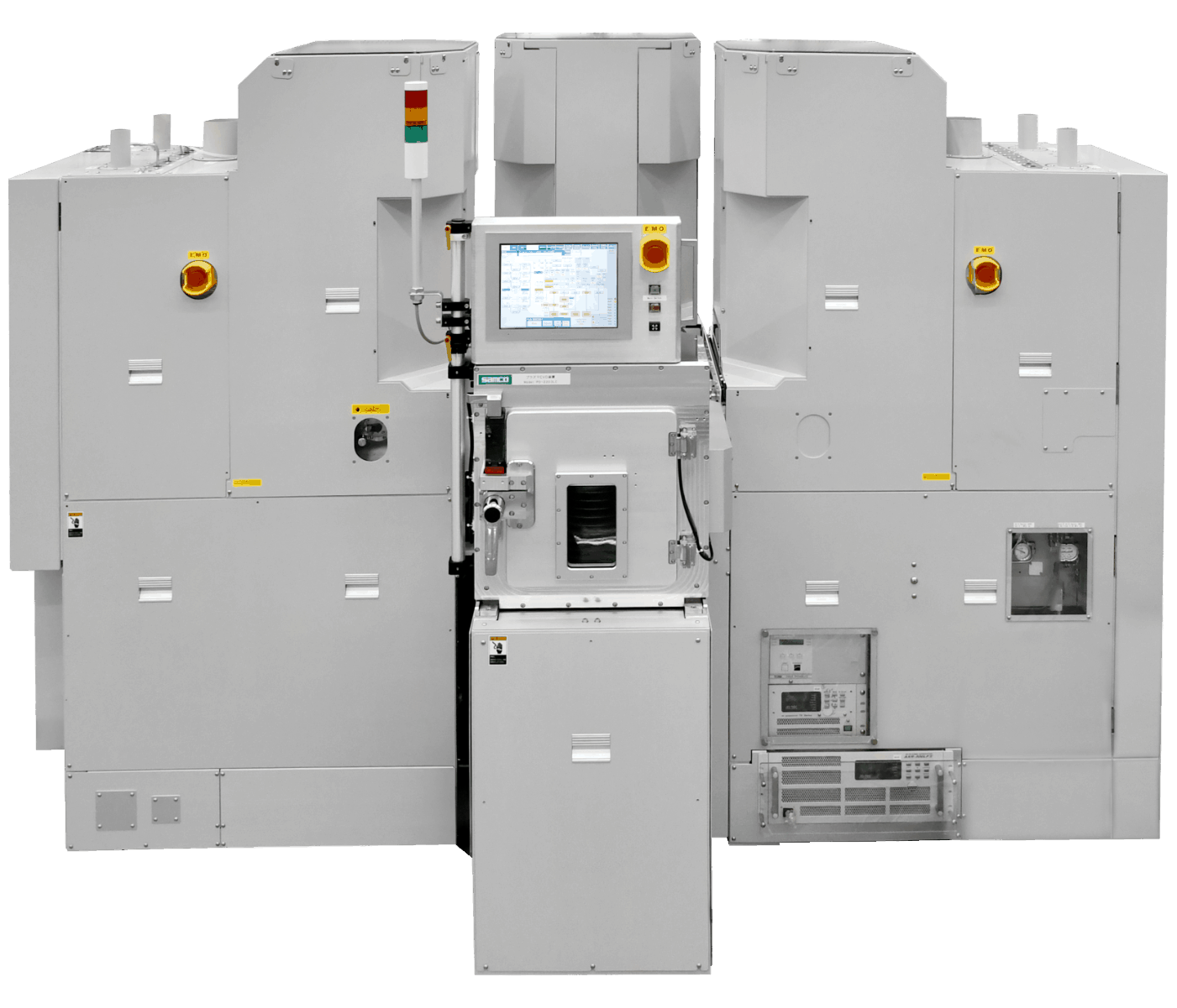
Samco’s AD-8002LPC dual-chamber ALD system enables stable TiOx deposition, reduced takt time, and flexible thermal and plasma ALD processing.
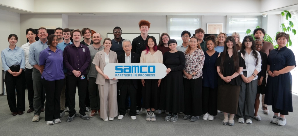
UCA students visit Samco to learn about semiconductors, plasma processing, Japanese business, and Samco’s founding story.
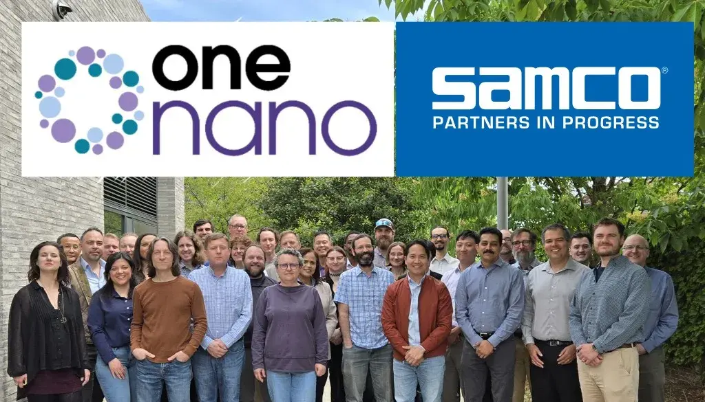
Samco presented ALE technologies at OneNano’s Spring Meredith Meeting, highlighting plasma-assisted etching for GaN HEMTs, diamond, and nanoscale devices.
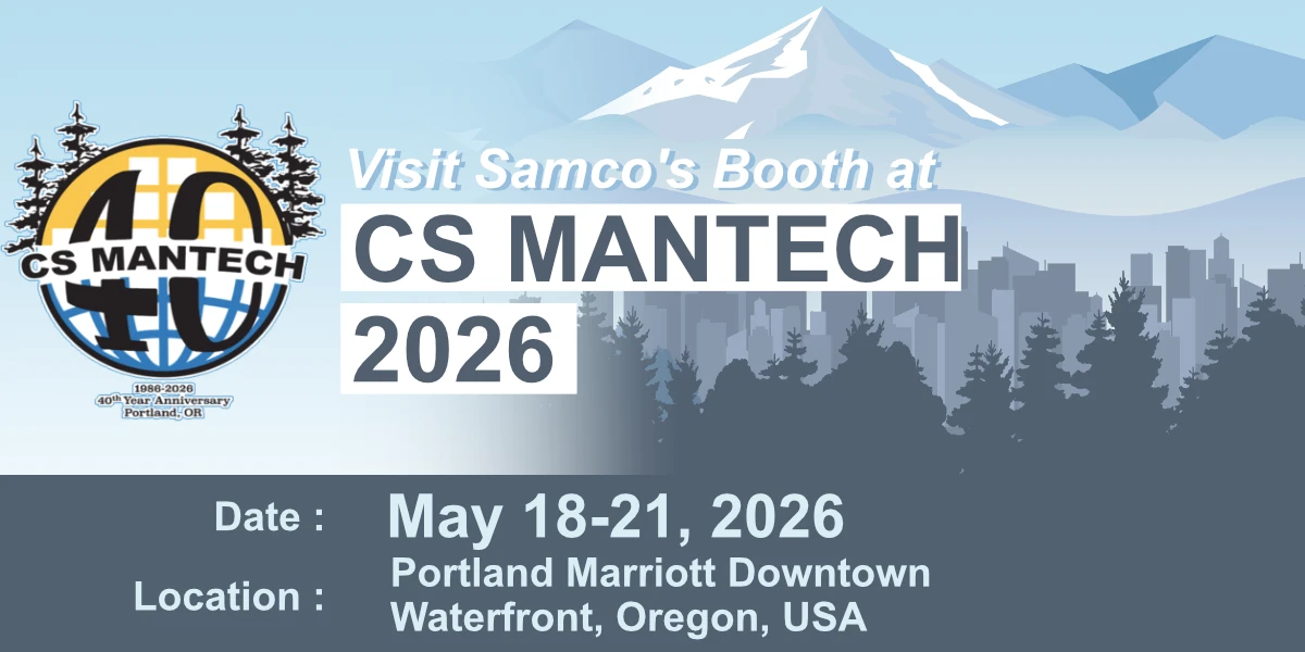
Samco Inc. will exhibit at CS MANTECH 2026, taking place from May 18–21, 2026, at the Portland Marriott Downtown Waterfront in Portland, Oregon.
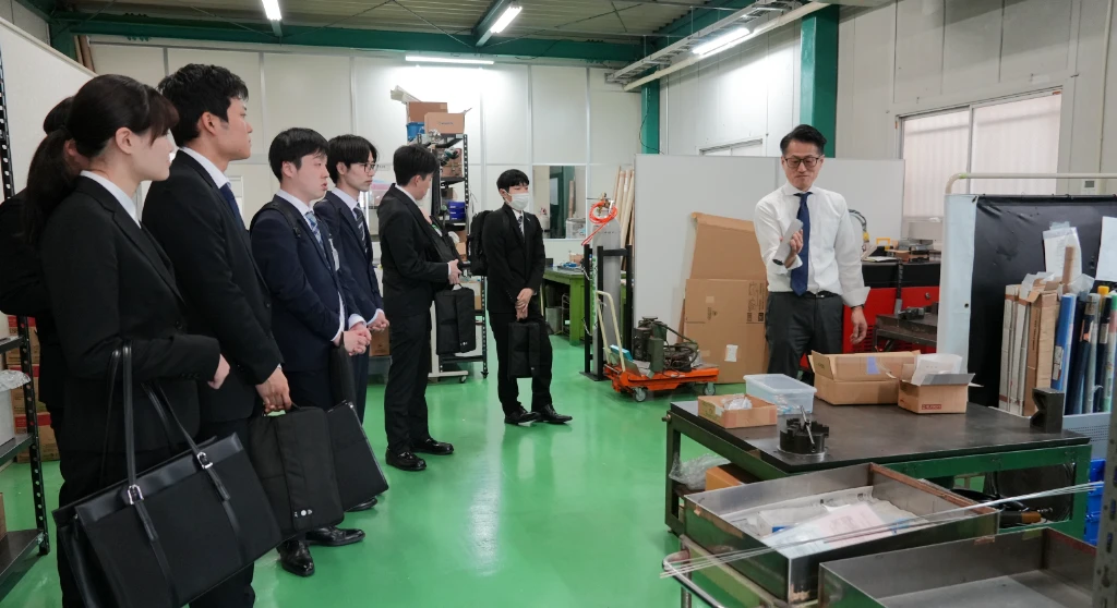
New employees visited Taisei Weld and Ushikoshi to learn how precision welding and metal fabrication support Samco’s semiconductor systems.
VCU EMBA students visited Samco in Kyoto, exploring its history, semiconductor manufacturing processes, and unique Kyoto approach to business and management.

Samco systems support IMiF’s GaN pilot line, enabling precise AlGaN/GaN etching and advancing wide bandgap semiconductor research in Europe.
GaN device isolation etching using ICP-RIE and endpoint detection enables uniform processing and stable multi-wafer semiconductor production.

The Technical University of Denmark selects Samco’s RIE-400iP plasma etching system for quantum photonics research, enabling precise III-V processing for single-photon device development.
Professor Kazunori Kataoka presents nanomachine-based drug delivery and the vision of “in-body hospitals” at the 2025 Samco Foundation lecture.
Samco expands partnership with ITRI Taiwan, focusing on semiconductor processing, silicon photonics, and chiplet integration through joint R&D efforts.
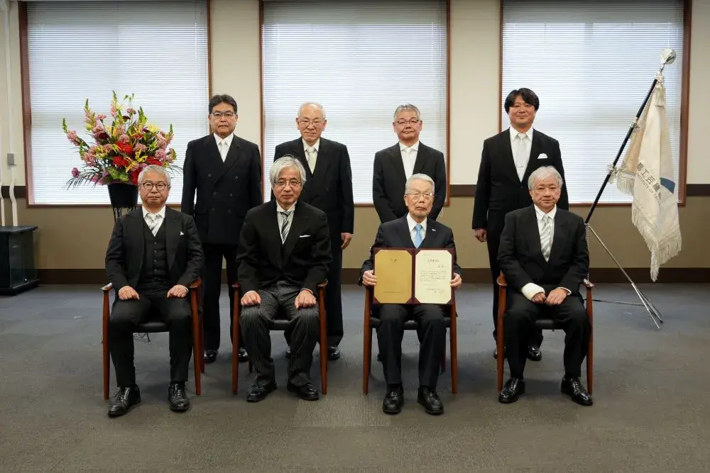
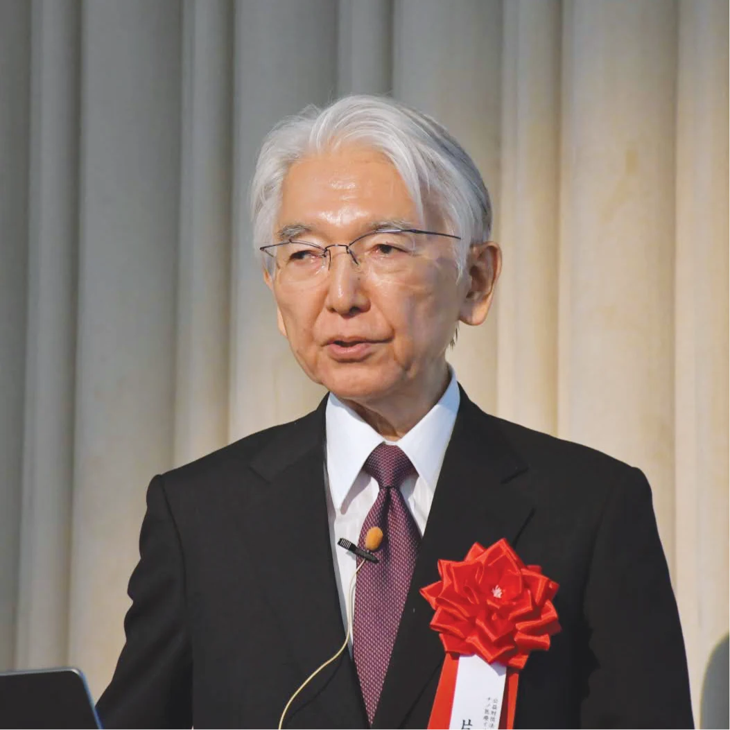
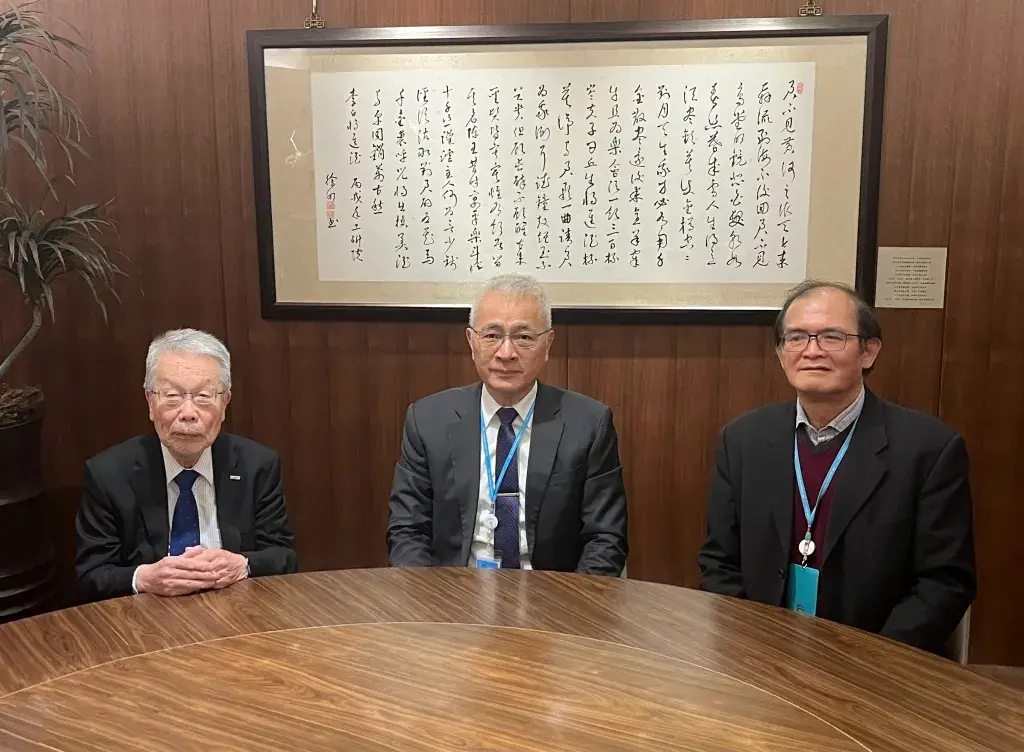
Samco Chairman Osamu Tsuji received an Honorary Doctorate from Kyoto Institute of Technology in recognition of his contributions to education and research.
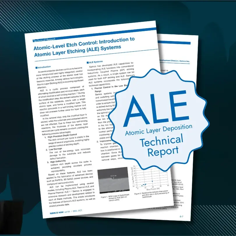
Introducing Samco’s Atomic Layer Etching (ALE) systems, detailing precise low-bias control and fast gas switching for uniform, low-damage etching processes.
Prof. Akiyoshi Baba shares insights on CMOS/MEMS research and managing Japan’s leading open-access semiconductor facility at Kyutech’s Iizuka Campus.
Samco’s RIE-400iP-ALE will become Australia’s first Atomic Layer Etching system, advancing III-V semiconductor and photonics research at the University of Adelaide.
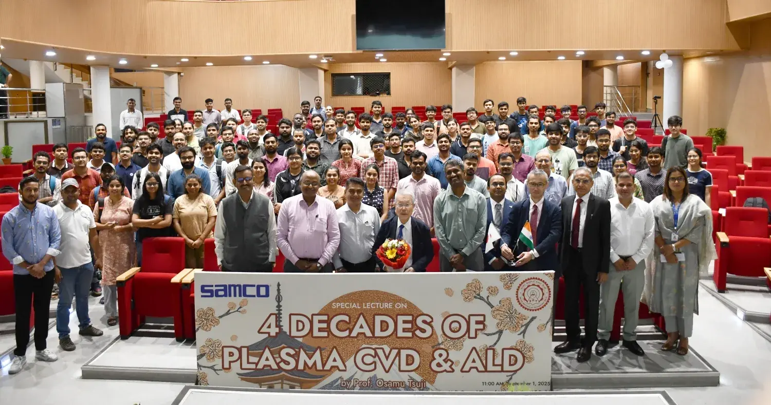
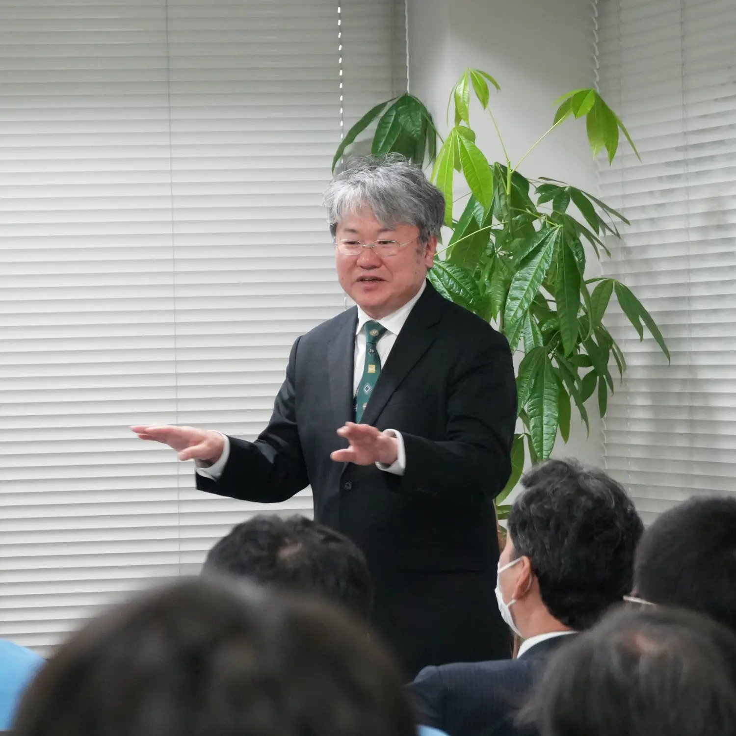
Samco founder Osamu Tsuji delivered an invited lecture at IIT Delhi on Plasma CVD, ALD, and the future of thin film technologies in semiconductor research.
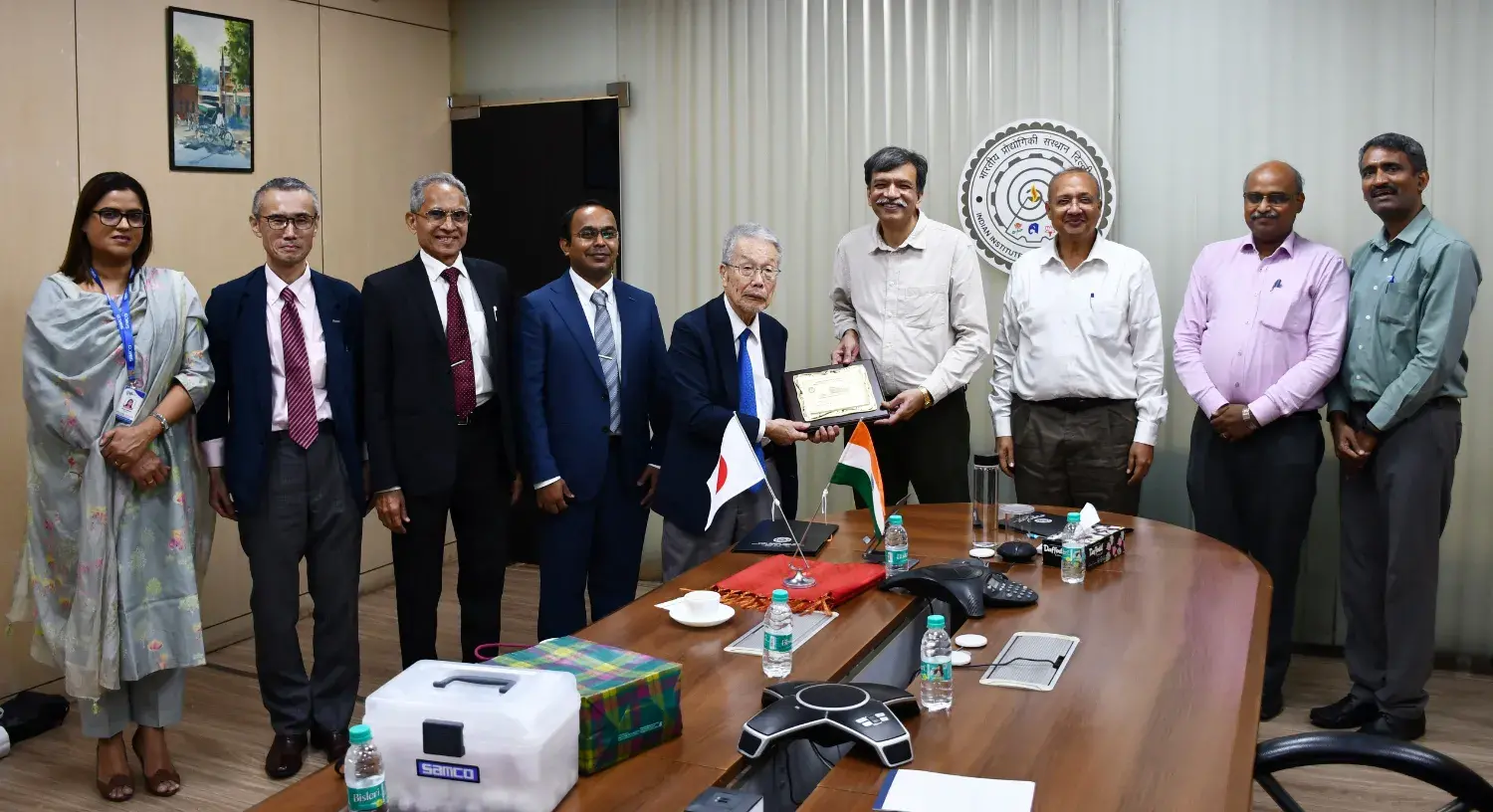
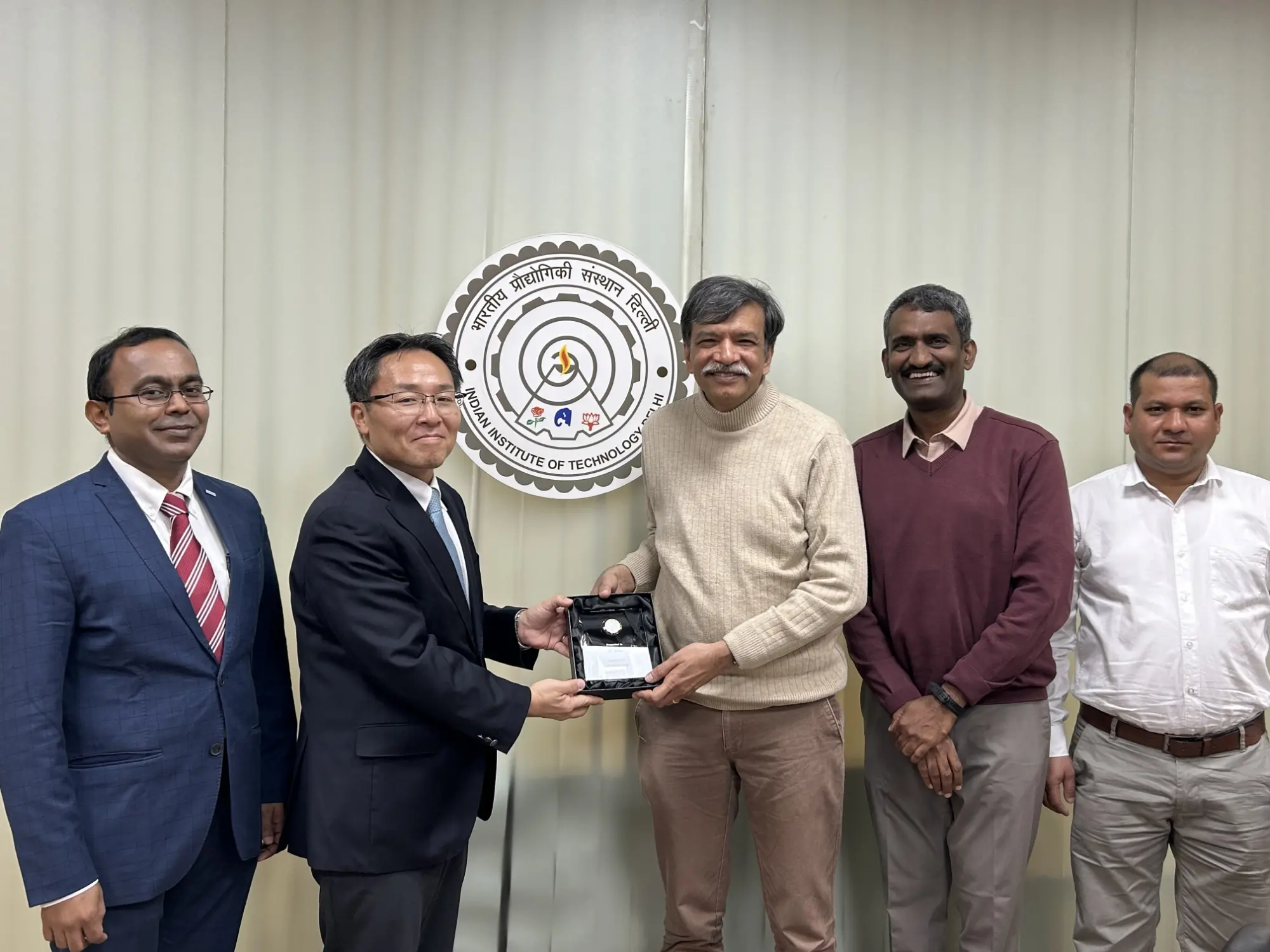
Samco signs an MoU with IIT Delhi to expand academic and research collaboration, supporting technology exchange and joint initiatives in advanced engineering.
PECVD System PD-200STL with anode/cathode switching allows for multitude of deposition conditions and demonstrates versatility of applications.
Samco opens its new Advanced Technology Development Center in Kyoto, featuring a Class 1,000 cleanroom to drive next-gen semiconductor innovation.
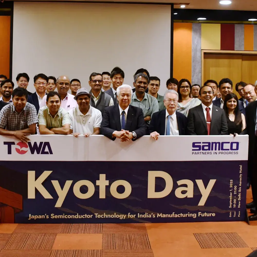
TOWA and Samco co-hosted Kyoto Day in New Delhi, sharing Japan’s semiconductor innovations to support India’s growing semiconductor industry.
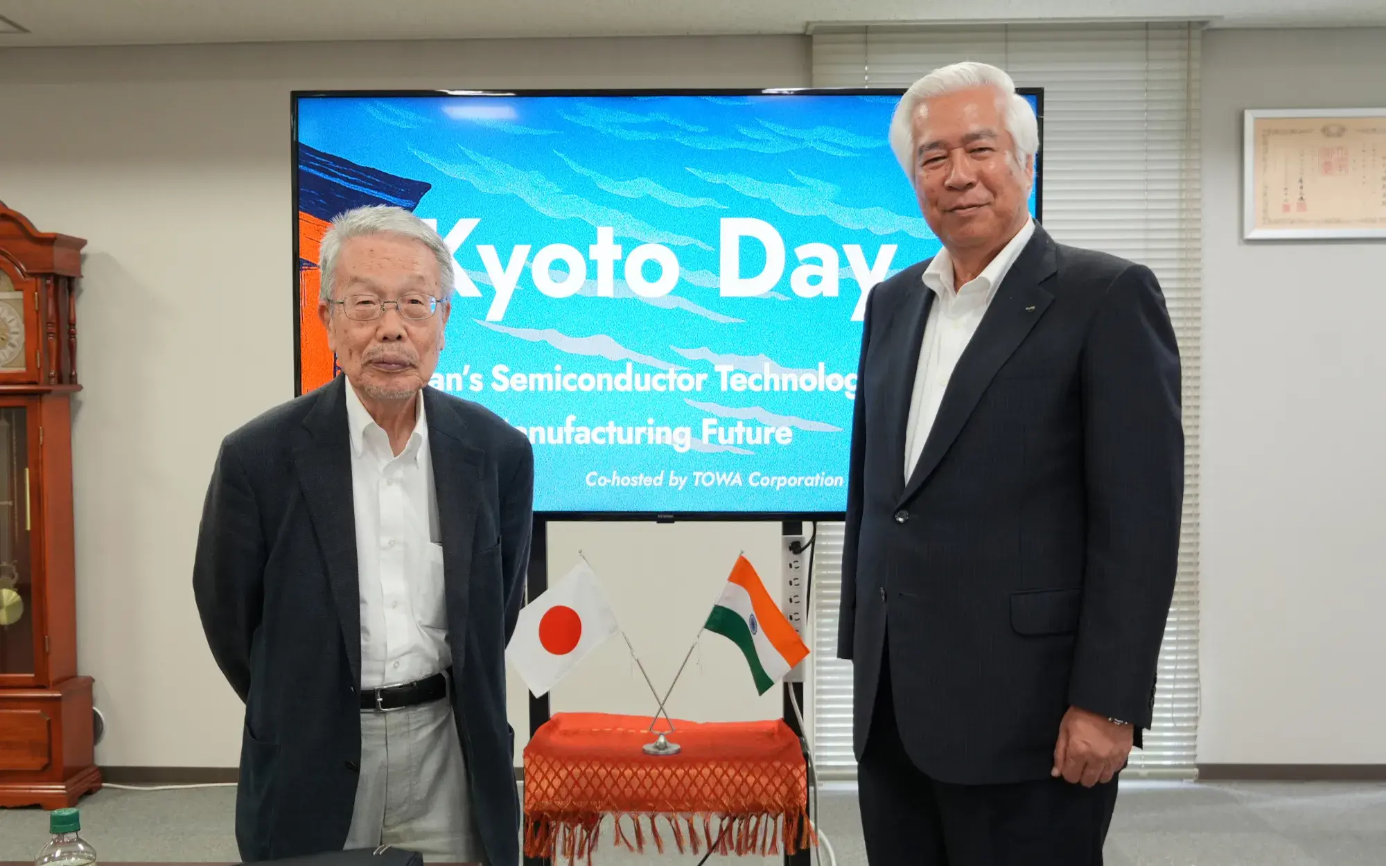
Kyoto Day in New Delhi brings TOWA and Samco together to showcase semiconductor innovations ahead of SEMICON India 2025.
Report investigating simultaneous dual-surface deposition of AlOx films on silicon wafers using the Plasma Enhanced Atomic Layer Deposition (PEALD) technique.
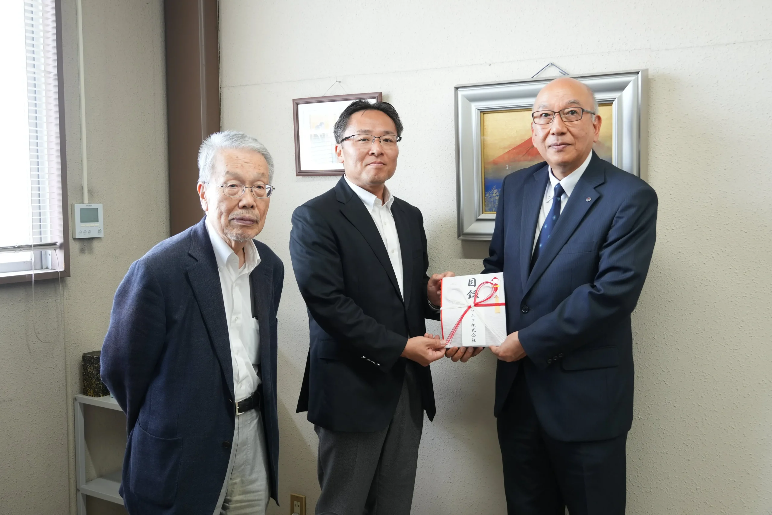
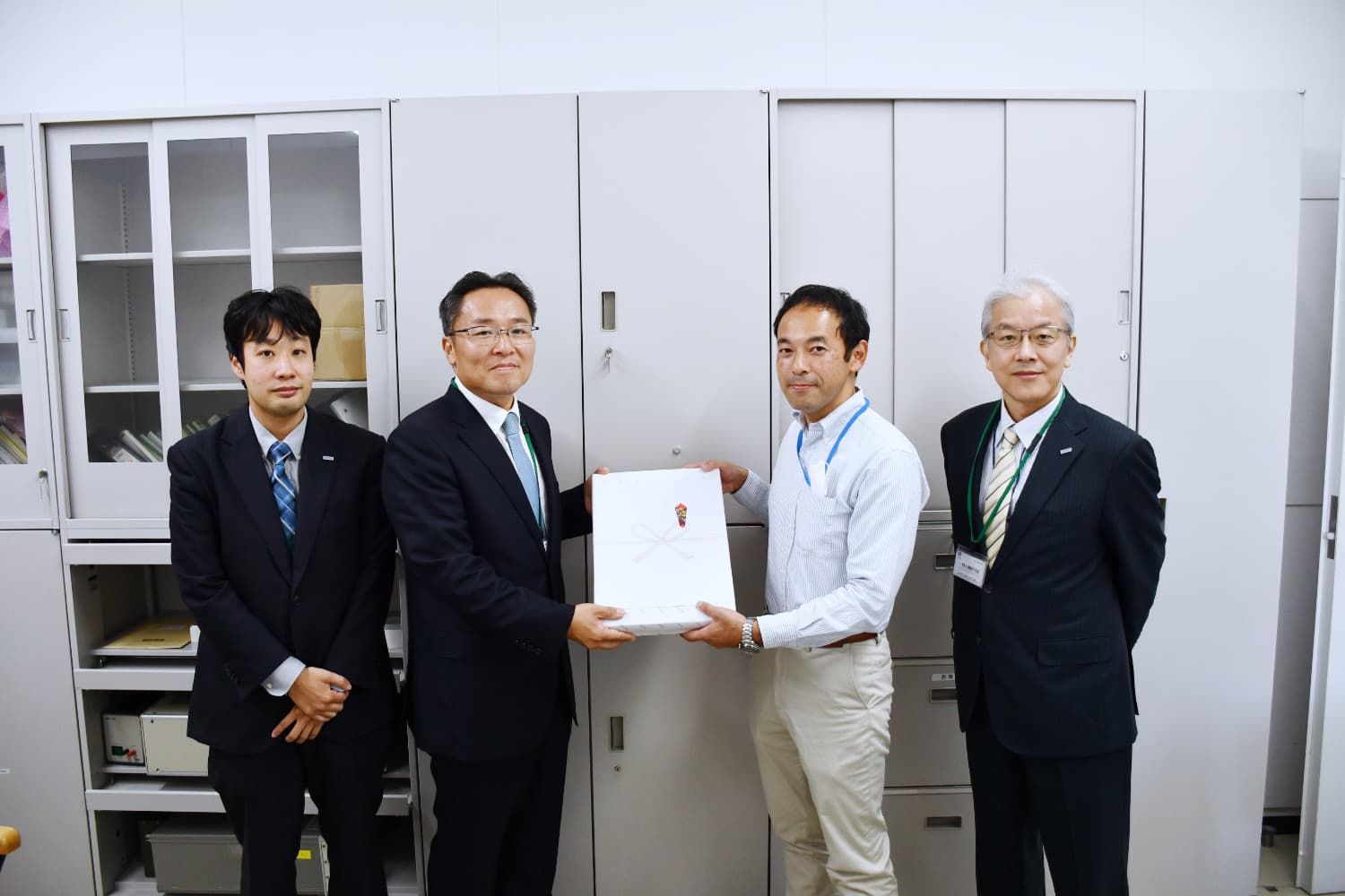
Samco Inc. donates 10 million JPY to the Japanese Red Cross Society, continuing its annual support for disaster relief and humanitarian efforts.
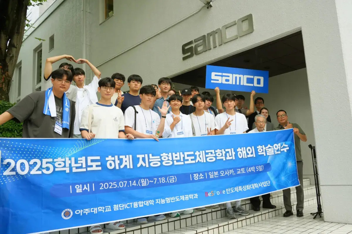
Ajou University students visit Samco for a hands-on look at semiconductor manufacturing and a Q&A session with CEO Osamu Tsuji during their Japan study tour.
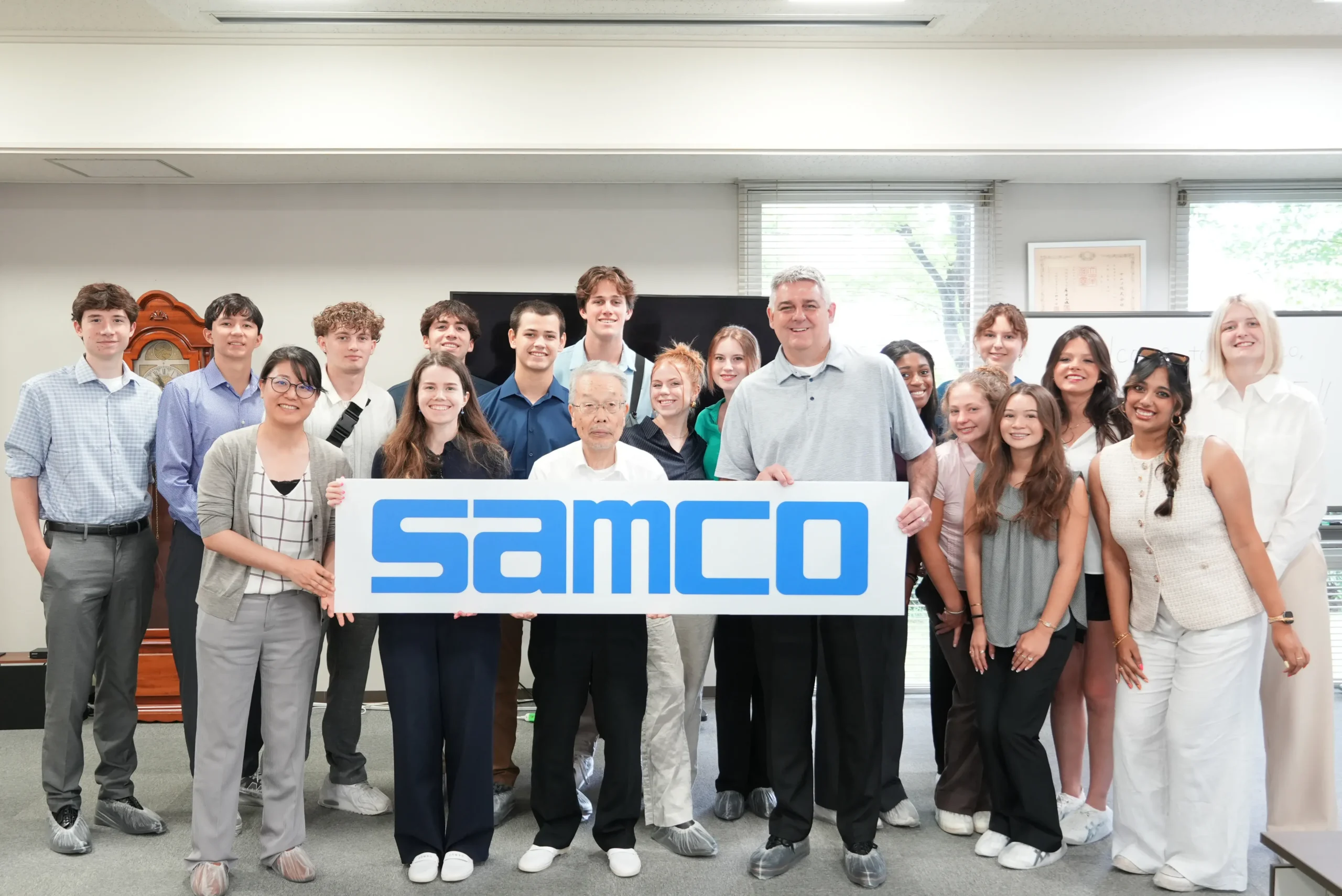
Samco welcomed Ohio State University students to Kyoto HQ. The students explored Samco’s history and learned about the semiconductor manufacturing field.
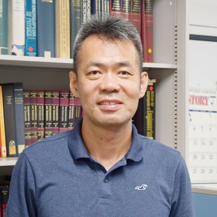
Advancing high-speed transistors with InP and GaN, Professor Yasuyuki Miyamoto explores the future of compound semiconductors and shares insights on Samco’s key role in research.
Professor Jun Suda of Nagoya University gave a special lecture at Samco on GaN devices, sharing insights on materials, processing, and future technologies.

TIME magazine features Samco’s journey from a Kyoto garage startup to a global semiconductor equipment leader in the article “Taking a Quantum Leap.”
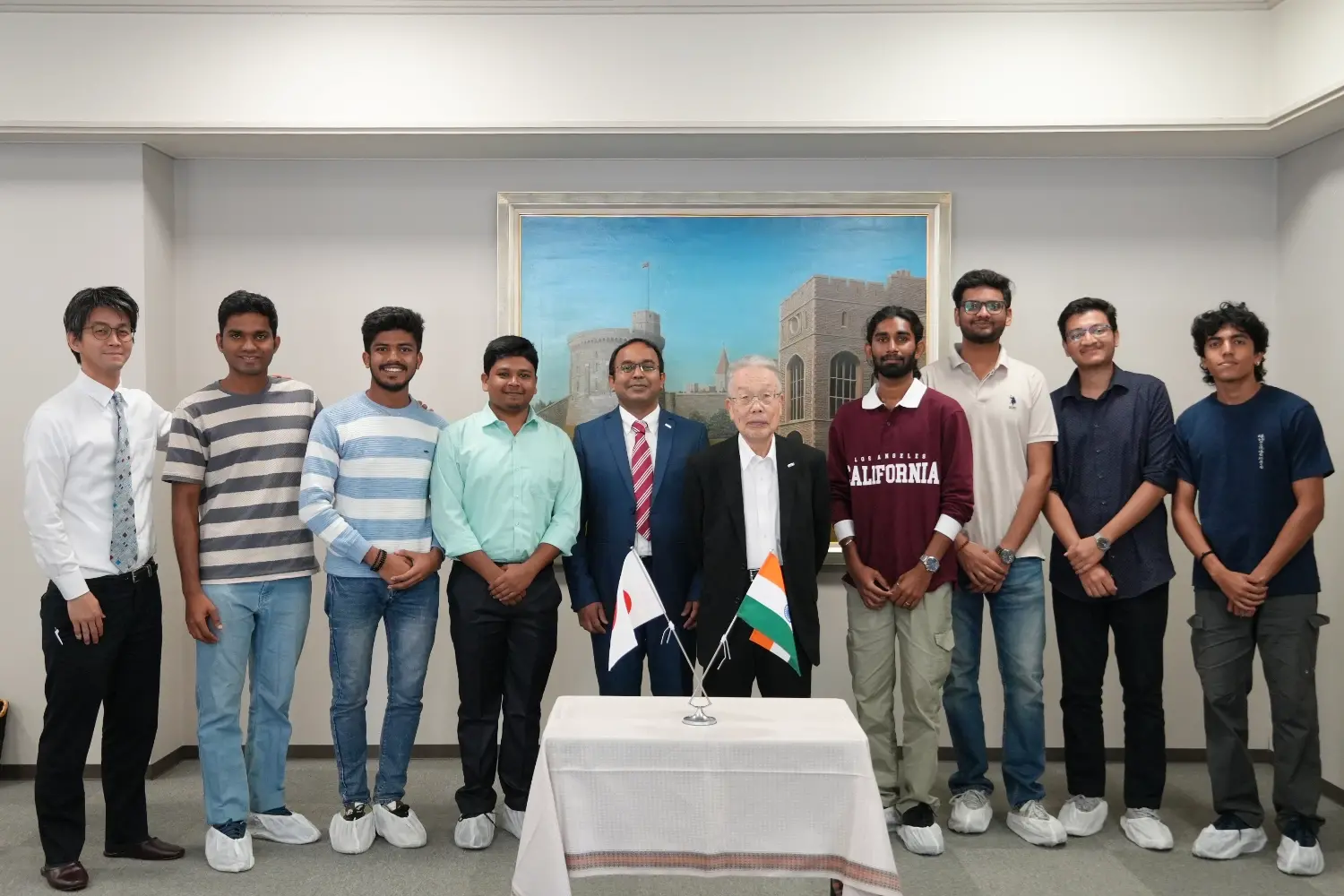
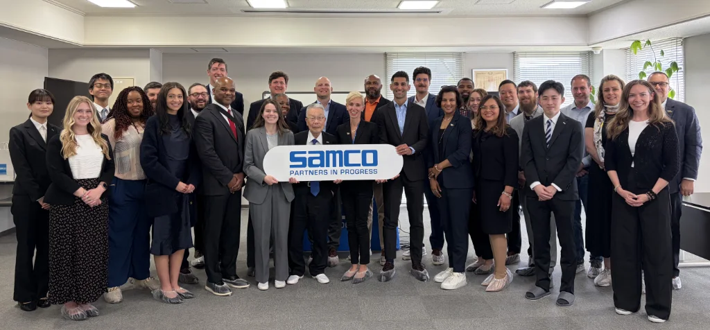
Samco welcomed KU-STAR Program students from top Indian universities for a factory tour, tech talk, and cultural exchange during their academic stay in Kyoto.
Research at Kyushu University explores next-gen display electronics, from AR/VR and micro-LEDs to retinal scanning and semiconductor devices.
Samco strengthens collaboration with IIT Delhi to advance Japan–India technology exchange, energy research, and talent development.
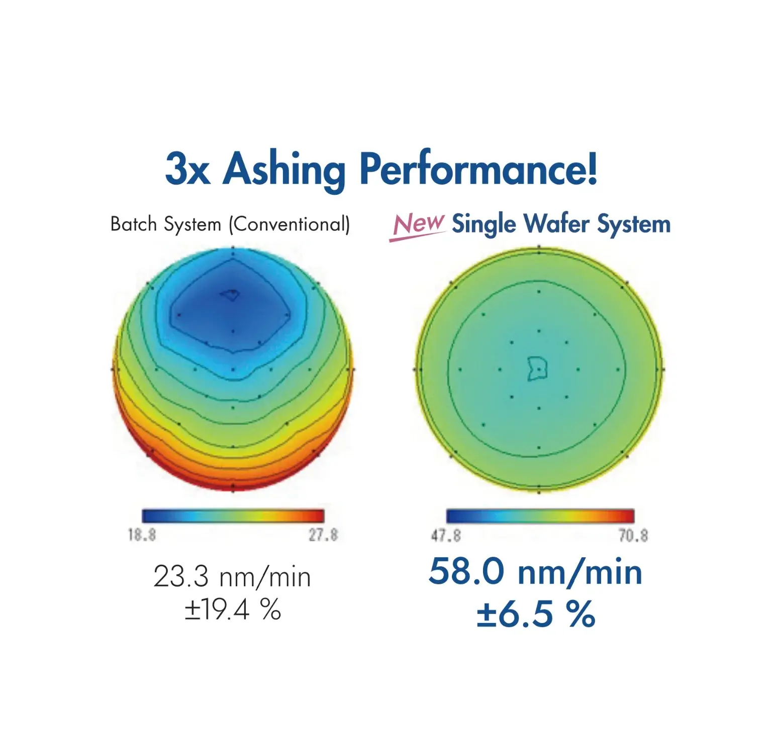
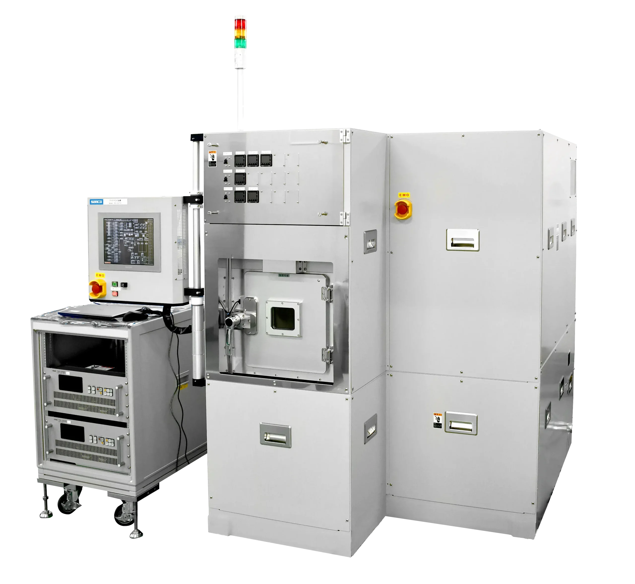
Samco’s single-wafer Aqua Plasma® system for wafer cleaning and descum processes, delivering improved ashing rates, uniformity, and throughput.
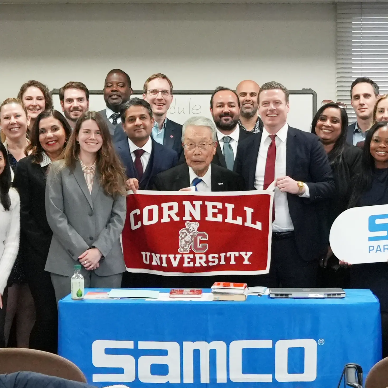
Cornell EMBA students visited Samco’s Kyoto headquarters to explore semiconductor innovation, leadership, and cross-cultural business insights.
MIT Professor Tomás Palacios visited Samco to discuss next-generation microelectronics, advanced materials, and potential research collaboration.
Samco introduces the PD-101TC PECVD system, enabling high-temperature thin film deposition up to 700°C for advanced semiconductor research.

Learn the fundamentals of Atomic Layer Deposition (ALD), a thin-film technique enabling atomic-scale thickness control, conformal coatings, and high-quality films.
Micro- and nanoscale device research, deposition and etching processes using RIE and PECVD for advanced structures.
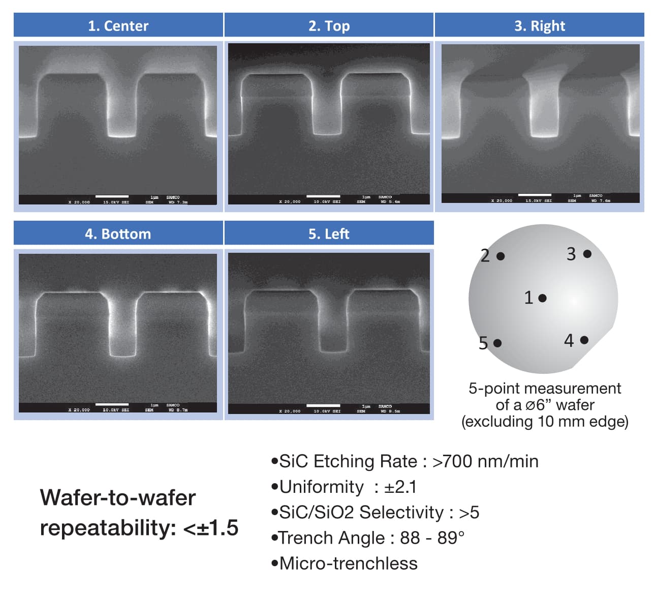
Advanced ICP trench etching for SiC MOSFETs achieving over 700 nm/min etch rates, rounded trench bottoms, and high uniformity on 6-inch wafers.
Research on silicon spin qubits for quantum computing, using PD-2201LC, RIE-400iPC, and RIE-230LC.
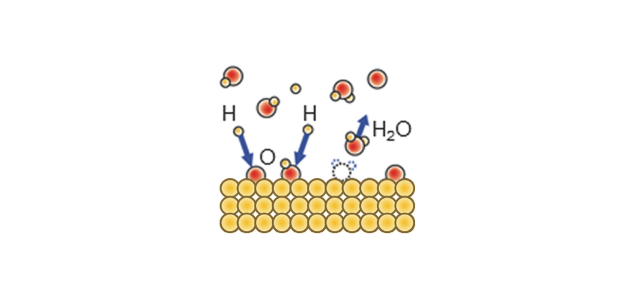
Learn how UV-ozone cleaning works, its advantages over plasma cleaning, and applications in semiconductor surface preparation and materials research.
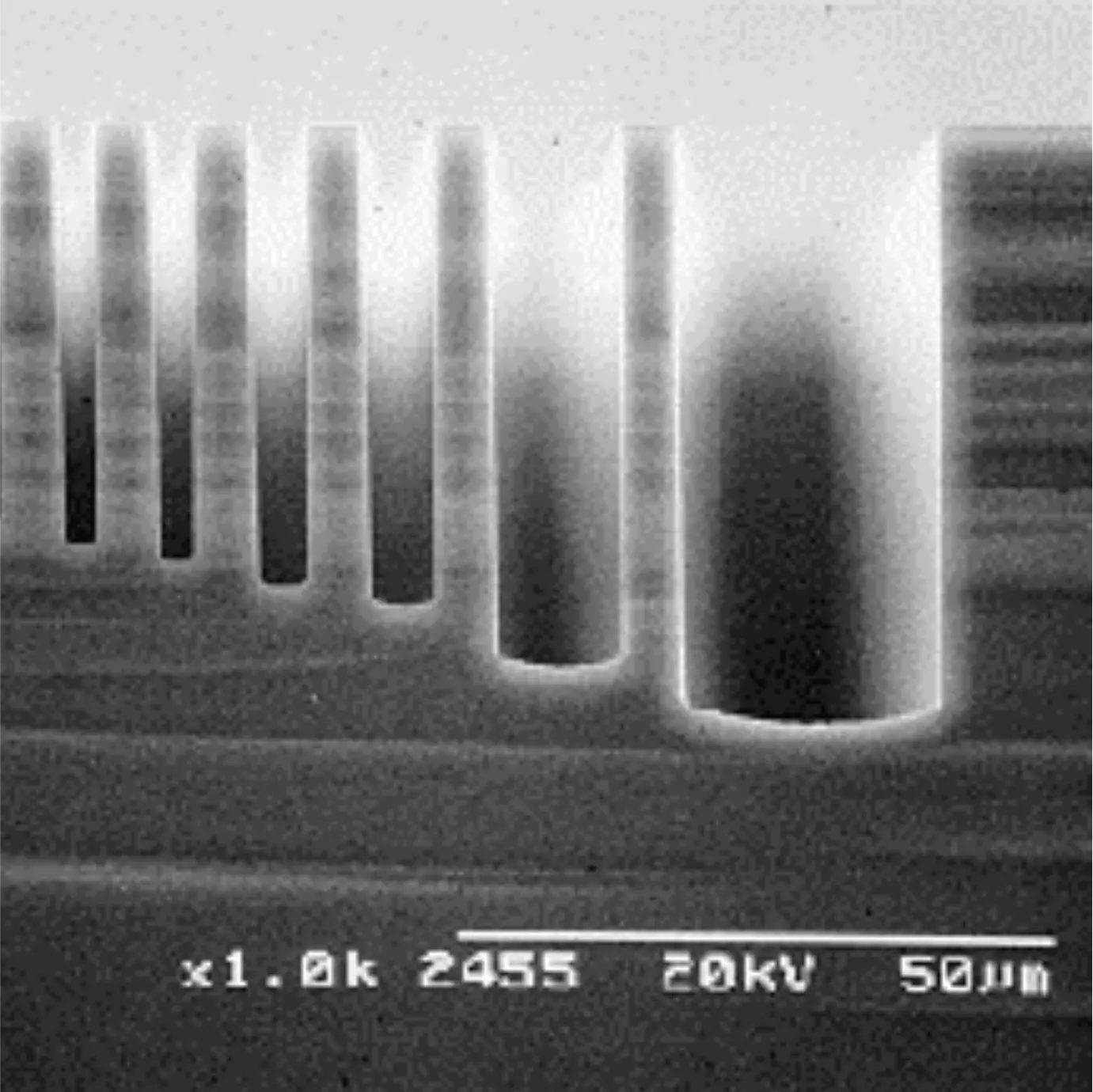
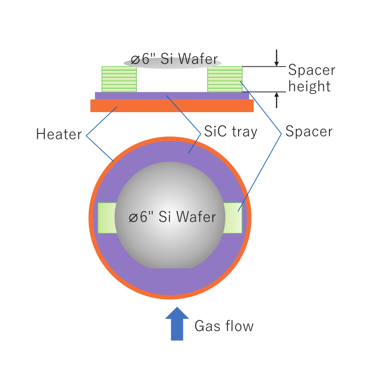
Explore loading and microloading effects in silicon DRIE and how process optimization improves etch uniformity and depth control in MEMS fabrication.
Aqua Plasma® treatment prevents oxidation, reduces gold surface oxides, and improves hydrophilicity for semiconductor manufacturing processes.
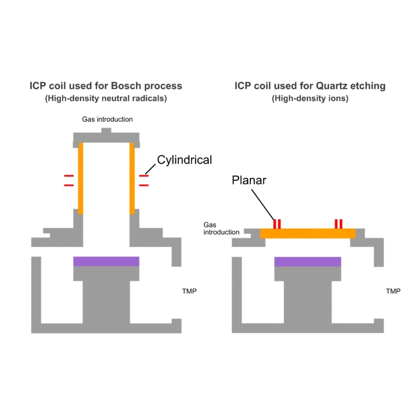
Learn key Bosch process hardware advances (including ICP source design, RF power control, fast gas switching, and pumping) to improve Si DRIE performance and profiles.
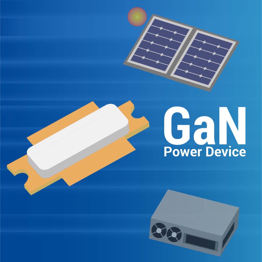
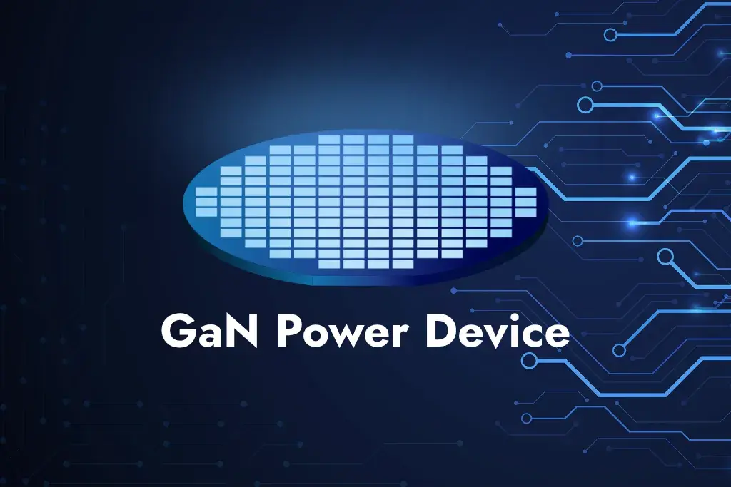
Key etching challenges in AlGaN/GaN power device fabrication and solutions for precise plasma etching of GaN-based semiconductor structures.
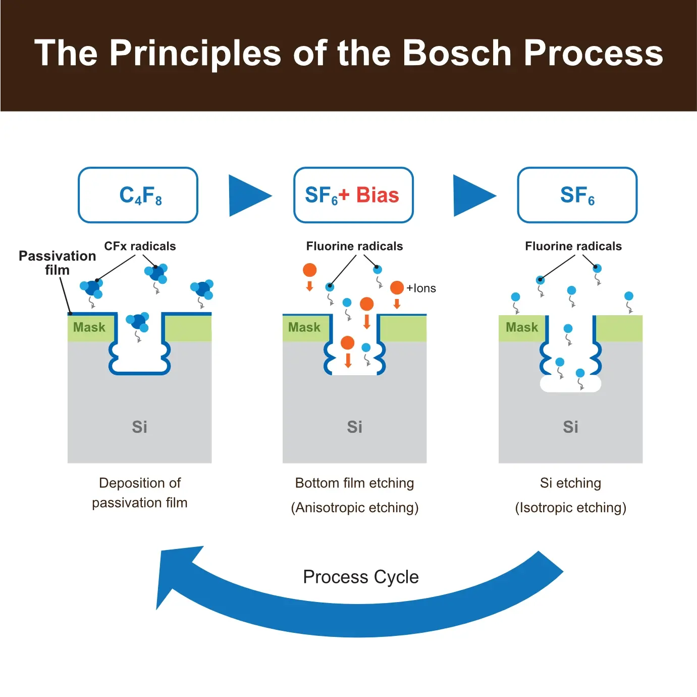
Learn how the Bosch process enables deep silicon DRIE with high aspect ratio features, using cyclic deposition and etching steps for anisotropic profiles and high selectivity.
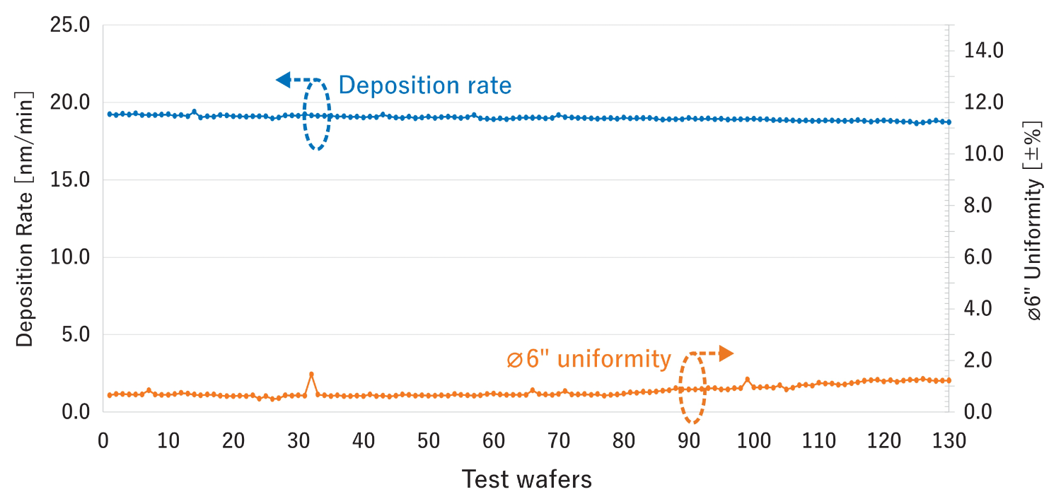
Long-term data shows stable SiN deposition using Samco’s PD-220 plasma CVD systems, maintaining ±2% uniformity over six months with reduced maintenance downtime.
Nanophotonics research, advanced applications, and the role of RIE-10NR in ICFO’s photonics projects.
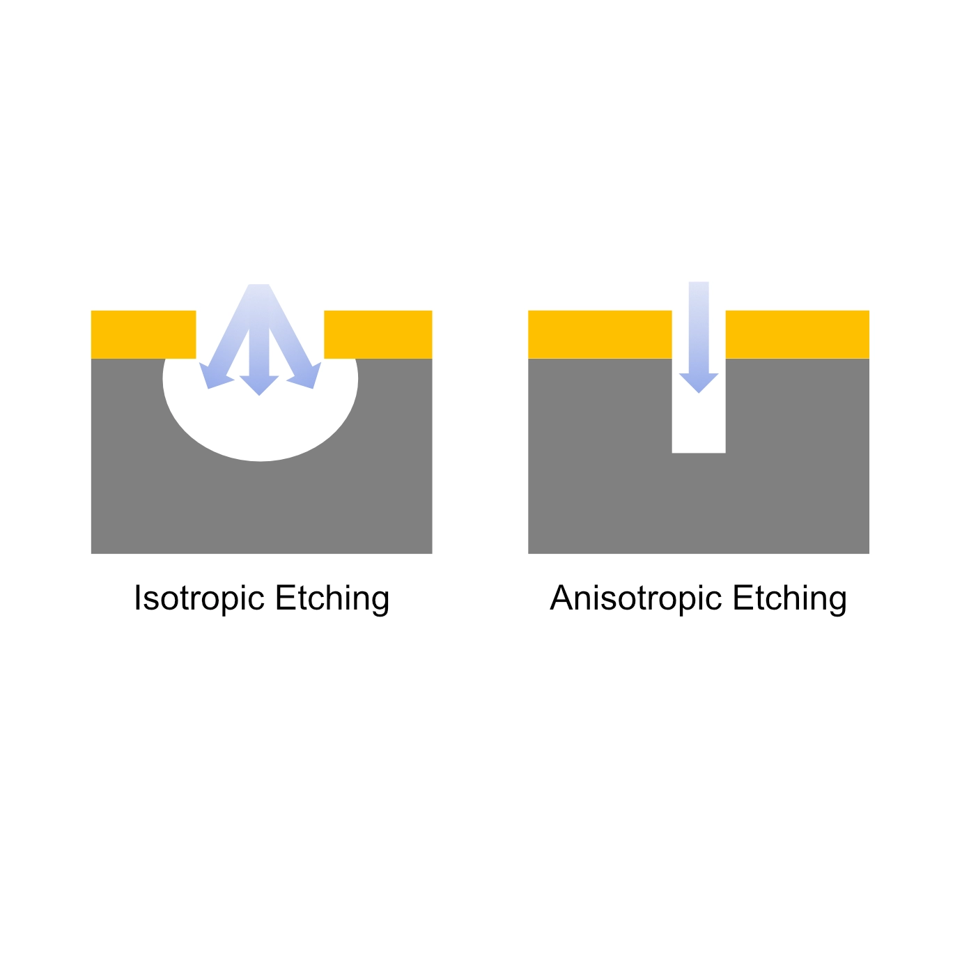
An introduction to Si DRIE, comparing Bosch, non-Bosch, and cryogenic processes and how Samco systems support MEMS, TSV, and packaging applications.
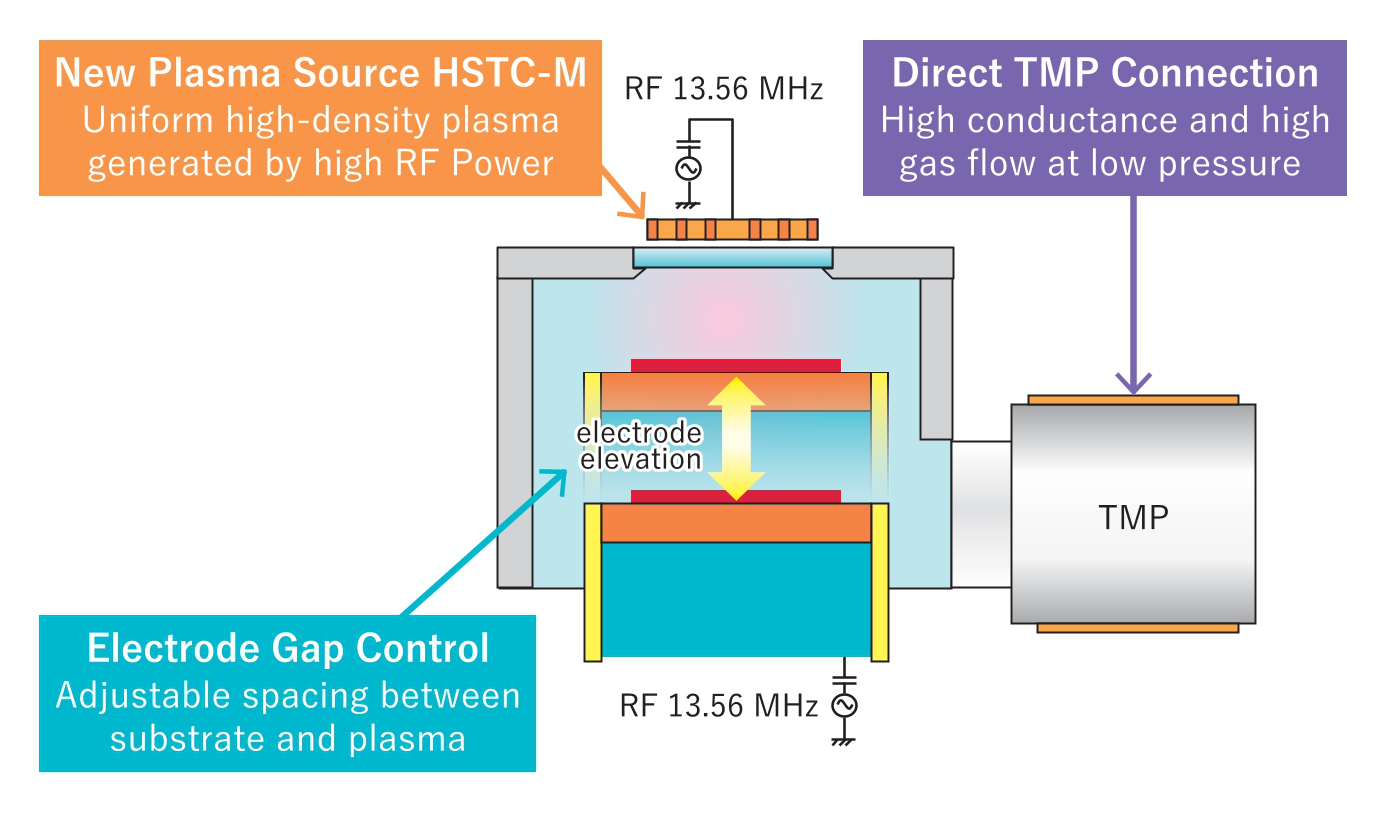
Samco introduces the HSTC-M™ plasma source for uniform, stable ICP etching of SiC and GaN power devices up to 8-inch wafers across research and production systems.
Optical metamaterials research, including nanostructures for light manipulation and high-sensitivity molecular detection, using Samco’s RIE-400iP.
Samco announces the sale of two RIE-400iP ICP-RIE systems to France-based III-V Lab to support advanced III-V semiconductor and silicon integration research.
Samco is featured in FORTUNE Businessweek on Kyoto’s semiconductor strength, highlighting Samco’s global growth, R&D expansion, and innovation rooted in Kyoto.
Bio-implantable microLED devices using RIE-200NL and PD-220NL systems.
Overview of three-chamber CVD system PD-2203LC, enabling stable SiN/SiO2 deposition with flexible frequency options for research and production.
Samco’s RIE-10NR CCP-RIE system surpasses 500 units shipped, marking a major milestone for a widely adopted etching tool in global research and development.
Research on Ga₂O₃ devices using RIE-200NL and other systems.
Samco and OST launch a partnership to support European R&D, providing RIE-10NR and UV-2 systems for microtechnology and photonics research in Switzerland.
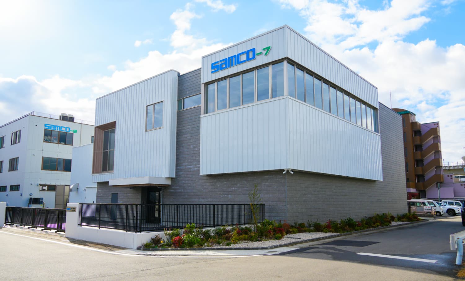
Samco announces plans to build a third R&D facility near its Kyoto headquarters, expanding cleanroom capacity to accelerate semiconductor equipment innovation.
Nano, micro-fabrication technology and materials development and thermal ALD for photochemistry.
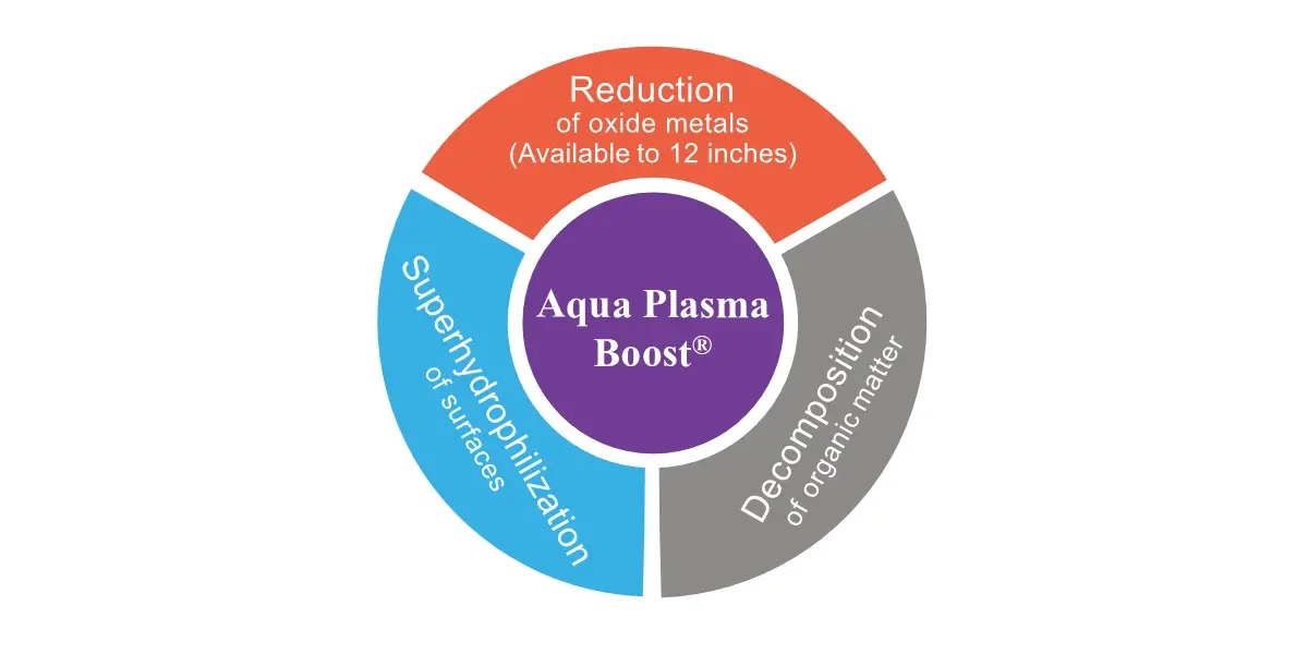
Samco developed Aqua Plasma Boost® to enhance oxidized copper reduction using reducing gas and water vapor.
Aqua Plasma® used for surface
modification of CO2 separation
nanomembranes.
Topological, diamond, and quantum nanophotonics, redefining light control and driving next-generation photonic innovation.
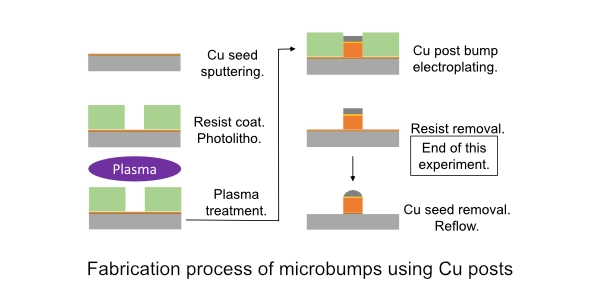
Samco’s Aqua Plasma® improves microbump fabrication by enhancing photoresist and Cu hydrophilization, preventing oxidation, and enabling better plating solution penetration for fine patterns.

A new trench-type SiC MOSFET fabrication approach combining ICP dry etching and ALD/PECVD gate insulators for improved breakdown and device performance.